
Index 129
74 Series digital circuit of 74LS362 four-phase clock generator / driver
Published:2011/8/1 22:56:00 Author:Lucas | Keyword: 74 Series , digital circuit , four-phase clock generator , four-phase driver

It is used as TMS9900 or other microprocessor clock generator/ driver; high four-phase output; complementary TTL four-phase output; it is the self-support oscillator controlled by the capacitor and crystal; it can connect external oscillator; the reset signal is synchronized by the clock D flip-flop with the Schmitt trigger input.
(View)
View full Circuit Diagram | Comments | Reading(1898)
74 Series digital circuit of 74LS354/356 8-to-1 data selector(tristate with address latching)
Published:2011/8/2 0:43:00 Author:Lucas | Keyword: 74 Series, digital circuit , 8-to-1 data selector, tristate , address latching
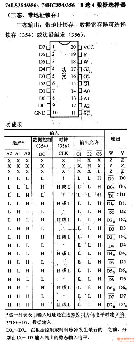
This list shows that the input address is established when the control is low. D1 ~ D7 are the data input. D0n ~ D7n are the steady state input level in D0 ~ D7 line before the latest increasing of the data control or clock pulse.
Three-state output with address latching; data register can choose data latch(354) or edge-triggered (356).
(View)
View full Circuit Diagram | Comments | Reading(842)
74 Series digital circuit of 74LS352, 74F352 dual 4-to-1 data selector(inverting)
Published:2011/8/1 20:49:00 Author:Lucas | Keyword: 74 Series , digital circuit , dual 4-to-1 , data selector, inverting
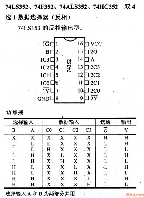
The selecting inputs A and B are used in common.
(View)
View full Circuit Diagram | Comments | Reading(881)
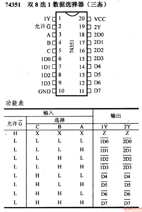
74 Series digital circuit of 74351 dual 8-to-1 data selector(tristate)
Published:2011/8/1 20:43:00 Author:Lucas | Keyword: 74 Series, digital circuit , dual 8-to-1 , data selector, tristate
View full Circuit Diagram | Comments | Reading(741)
74 Series digital circuit of 74LS299, 74S299 8-bit bidirectional universal shift/storage registers
Published:2011/8/2 4:36:00 Author:Lucas | Keyword: 74 Series , digital circuit , 8-bit bidirectional, universal shift, storage registers
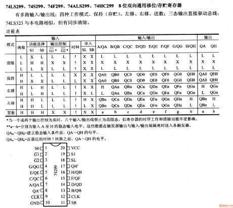
It has multi-road / output lines and four modes to maintain (store) left, right shift and output number; three-state outputs can directly drive the bus; 74LS323 is similar to the circuit, but it has the synchronous clear function. When one or two output controlling is high, eight input / output ends against in high-impedance state, but the timing register and cleaning functions are not affected. The data is input to each trigger when the flip-flop output and input ends are isolated.
QA10~QH0 is the level of QA~QH before the establishment of steady-state input conditions. QAn~QHn=the level of QA~QH before the latest time hopping.
(View)
View full Circuit Diagram | Comments | Reading(1722)
74 Series digital circuit of 74LS323,74S323 8-bit bidirectional universal shift/storage registers
Published:2011/8/2 4:34:00 Author:Lucas | Keyword: 74 Series, digital circuit , 8-bit bidirectional , universal shift, storage registers
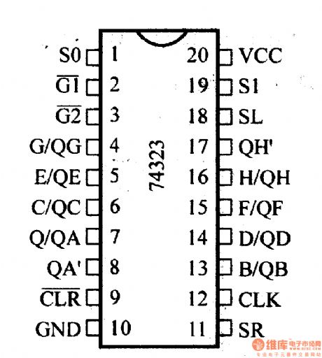

It has multi-road / output lines and four modes to maintain (store) left, right shift and output number; three-state outputs can directly drive the bus; 74LS299 is similar to the circuit, but it has the asynchronous reset. When one or two output controlling is high, eight input / output ends against in high-impedance state, but the timing register and cleaning functions are not affected. The data is input to each trigger when the flip-flop output and input ends are isolated.
QA10~QH0 is the level of QA~QH before the establishment of steady-state input conditions. QAn~QHn=the level of QA~QHbefore the latest timehopping.
(View)
View full Circuit Diagram | Comments | Reading(962)
74 Series digital circuit of 74LS322,74F322 sign-extended 8-bit shift register
Published:2011/8/2 3:55:00 Author:Lucas | Keyword: 74 Series, digital circuit , sign-extended 8-bit , shift register
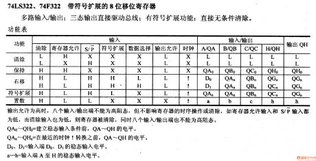
Multiple input / output; tri-state outputs can directly drive the bus; it has signed extended function; it can be direct unconditional cleared. When the output allows for high, eight input / output ends can not be in a high-impedance state, but does not affect the timing operation or clear of registers, for example, if the register allows the input and S / P input, the clear input are low, the register is removed, and eight input / output ends can not be in a high-impedance state.
QA0 ...QH0= QA ...QH level before the establishment of steady-state input conditions.
D0, D1=the steady input level ofinput ends D0, D1
a..h =the steady input level of the input ends of A to H.
(View)
View full Circuit Diagram | Comments | Reading(849)
74 Series digital circuit of 74LS295B 4-bit bidirectional universal shift register (tristate)
Published:2011/8/2 4:24:00 Author:Lucas | Keyword: 74 Series , digital circuit , 4-bit bidirectional , universal shift register , tristate
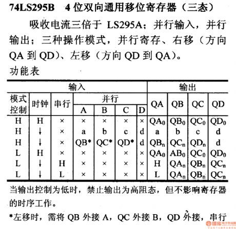
Absorption current is three times greater than LS295A; parallel input, parallel output; it has three operation modes with parallel register, and the right shift(direction is from QA to QD), left shift(the direction is from QD to QA). Data is input at the D-side.
a, b, c, d = the corresponding steady input level of A, B, C, D.
QA0, QB0, QC0, QD0= the corresponding level of QA, QB, QC, QD before the establishment of steady-state input conditions.
QAn, QBn, QCn= the corresponding level of QA, QB, QC at the latest time hopping.
(View)
View full Circuit Diagram | Comments | Reading(1265)
74 Series digital circuit of 74LS294,74HC294 programmable divider / digital timer
Published:2011/8/1 20:44:00 Author:Lucas | Keyword: 74 Series , digital circuit , programmable divider , digital timer
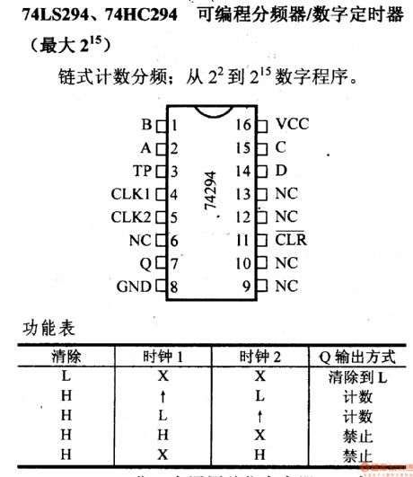
View full Circuit Diagram | Comments | Reading(1094)
74 Series digital circuit of 74LS292,74HC292 programmable divider / digital timer
Published:2011/8/1 20:45:00 Author:Lucas | Keyword: 74 Series , digital circuit , programmable divider , digital timer
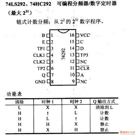
View full Circuit Diagram | Comments | Reading(1007)
74 Series digital circuit of 74285 4 × 4-bit parallel binary multiplier(low topological product)
Published:2011/8/1 20:24:00 Author:Lucas | Keyword: 74 Series , digital circuit , 4 × 4-bit parallel , binary multiplier, low topological product
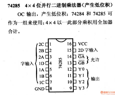
OC output can generate low topological product; 74284 and 74285 can be used in a group. 4 × 4-this part of the product is combined with a full adder.
(View)
View full Circuit Diagram | Comments | Reading(2179)
74 Series digital circuit of 74284 4 × 4-bit parallel binary multiplier(high topological product)
Published:2011/8/1 20:21:00 Author:Lucas | Keyword: 74 Series , digital circuit , 4 × 4-bit parallel , binary multiplier, high topological product
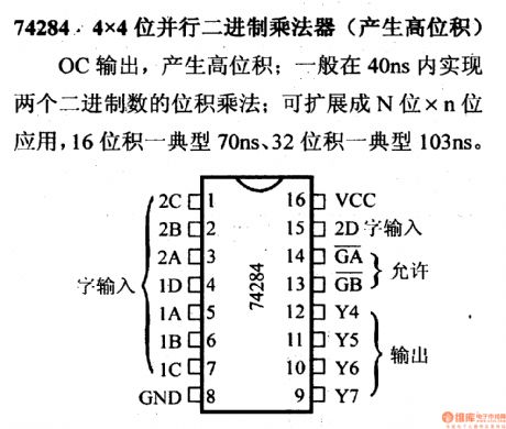
OC output can generate topological product; it typically realizes two binary numbers topological product multiplication in 40ns; it can be extended to N-bit × n-bit application, 16-bit product - typical 70ns, 32-bit product - typically 103ns.
(View)
View full Circuit Diagram | Comments | Reading(1950)
74 Series digital circuit of 74278 4-bit cascade priority register(controllable output)
Published:2011/8/1 20:46:00 Author:Lucas | Keyword: 74 Series , digital circuit , 4-bit cascade, priority register, controllable output
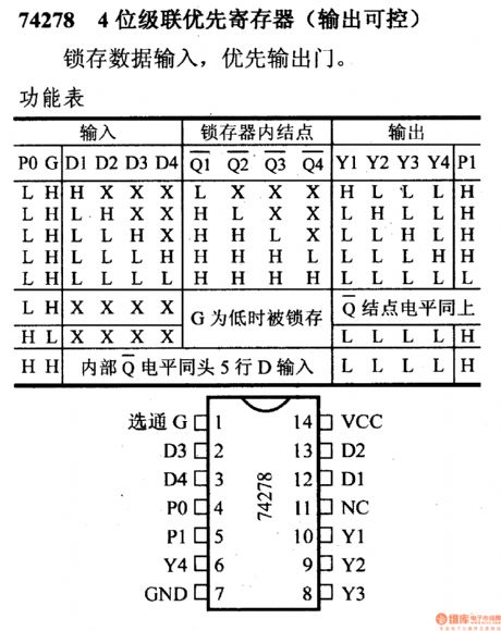
View full Circuit Diagram | Comments | Reading(758)
74 Series digital circuit of 74S274 4 × 4-bit binary multiplication (tristate)
Published:2011/8/1 23:55:00 Author:Lucas | Keyword: 74 Series , digital circuit , 4 × 4-bit , binary multiplication , tristate
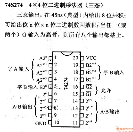
Three-state output; it has given 8-bit product in 45ns (typical); it can be given n-bit × n-bit binary numbers factor product; when any one (or two) G input is high, all eight outputs are deadline.
(View)
View full Circuit Diagram | Comments | Reading(1414)
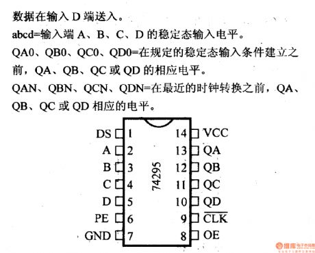
74 Series digital circuit of 74259,74LS259 8-bit addressable latch
Published:2011/8/2 0:51:00 Author:Lucas | Keyword: 74 Series , digital circuit, 8-bit addressable latch
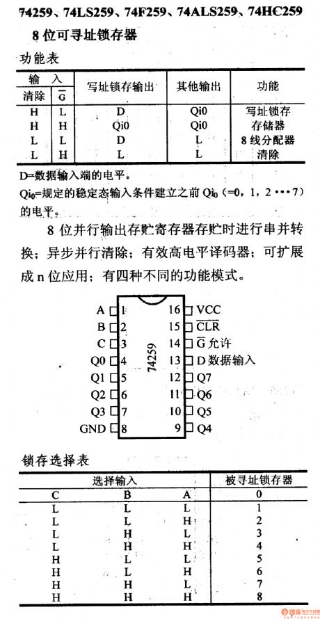
D=the level of the data input end.
Qio = the output level before establishing the steady-state input conditions.
8-bit parallel output storage register can make serial parallel conversion; asynchronous parallel clear; active high decoder; it can be extended to n-bit applications; it has four different function modes.
(View)
View full Circuit Diagram | Comments | Reading(2001)
74 Series digital circuit of 74248,74249 BCD seven segment decoder / driver
Published:2011/8/2 4:17:00 Author:Lucas | Keyword: 74 Series , digital circuit , BCD seven segment , decoder , driver

It can drive the effective high level output of light buffer; it has lamp test device; frontier, back porch are zero out; it can adjust the light intensity; 248 contains the boost resistor; 249 is the collector open circuit output, and the pin diagram is the same with 74246.
1. It requires 0 to 15, then the turning off input (BI) must remain high level, if it does not eliminate decimal zero, the dynamic turning off input (RBI) is open or high. If the low input is direct added to turning off input, all segment outputs are off regardless of the level of other inputs.
(View)
View full Circuit Diagram | Comments | Reading(2011)
74 Series digital circuit of 74246,74247 BCD seven segment decoder / driver
Published:2011/8/2 4:13:00 Author:Lucas | Keyword: 74 Series , digital circuit , BCD seven segment , decoder , driver
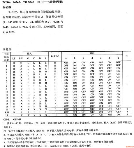
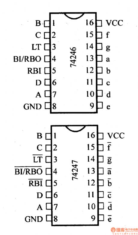
The open-collector output can directly drive the display; it has lamp test device; frontier, back porch are zero out; it can adjust the light intensity; the withstand voltage of 246 is 30V, and the withstand voltage of 247 is 15V; the 74246 and 7446,74247,7447 are similar but the word shapes, thus they are interchangeable. 1. It requires 0 to 15, then the turning off input (BI) must remain high level, if it does not eliminate decimal zero, the dynamic turning off input (RBI) is open or high. If the low input is direct added to turning off input, all segment outputs are off regardless of the level of other inputs.
(View)
View full Circuit Diagram | Comments | Reading(6169)
Typical application circuit of 5G168 holiday lights control IC
Published:2011/8/7 21:16:00 Author:Ecco | Keyword: Typical application, holiday lights , control IC
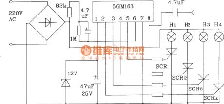
In the circuit, pin 9, 10 are floating to drive four ways of lights for Love-style jump. Changing external R, C size of pin 6 can change the frequency of flashing lights. If the pin 8 is input audio signal, the lights' cycle will change with the audio AC signal.
(View)
View full Circuit Diagram | Comments | Reading(649)
Low-frequency FM generator circuit composed of two NE566V ICs
Published:2011/8/8 8:02:00 Author:nelly | Keyword: Low-frequency, FM, generator

As shown in the picture, two NE566V ICs form the low-frequency FM generator. In the picture, ICl NE566V is used to produce the signal, and IC2 works on the carrier signal. Ctl can be selected to determine the modulation frequency range. The Ct2 can be selected to determine the core frequency. The output modulation can use the Sl to choose the square wave and triangular wave, thus the square wave modulation and triangular wave modulation can be achieved. (View)
View full Circuit Diagram | Comments | Reading(1028)
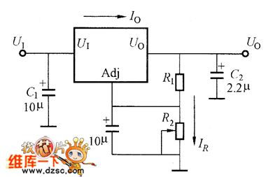
The basic application circuit diagram of LT108X adjustable voltage regulator
Published:2011/8/7 6:27:00 Author:nelly | Keyword: adjustable voltage regulator
View full Circuit Diagram | Comments | Reading(975)
| Pages:129/471 At 20121122123124125126127128129130131132133134135136137138139140Under 20 |
Circuit Categories
power supply circuit
Amplifier Circuit
Basic Circuit
LED and Light Circuit
Sensor Circuit
Signal Processing
Electrical Equipment Circuit
Control Circuit
Remote Control Circuit
A/D-D/A Converter Circuit
Audio Circuit
Measuring and Test Circuit
Communication Circuit
Computer-Related Circuit
555 Circuit
Automotive Circuit
Repairing Circuit