
Index 139
BANDPASS_FOB_85O_Hz_RTTY_SHIFT
Published:2009/7/15 1:55:00 Author:Jessie
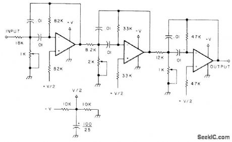
Three-stage active Butterworth input filter passes 2125- and 2975-Hz tones plus modulation side-bands and allowance for drift in RTTY receiver. Inset shows how 741 opamps are biased when used with single power supply. Article gives step-by-step design and alignment procedures.-P. A. Stark, Design an Active RITY Filter, 73 Magazine, Sept. 1977, p 38.-43. (View)
View full Circuit Diagram | Comments | Reading(1134)
CLOCK_FOR_TEST_MESSAGES
Published:2009/7/15 1:54:00 Author:Jessie
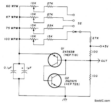
Generates negative going pulse train at choice of four baud rates, to control RTTY test-message generator at four different speeds.-K. Ebneter and J. Romelfanger, RTTY Test-Message Generator, Ham Radio, Nov. 1976, p 30-32. (View)
View full Circuit Diagram | Comments | Reading(643)
RING_COUNTER_FOR_3_PHASE_INVERTER
Published:2009/7/15 1:54:00 Author:Jessie
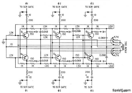
Supplies control signals for all three phases in correct sequence, working from symmetrical Hartley 1,200-cps oscillator,Uses three fip-flops.-M. Lilienslein, Static Inverler Delivers Regulated 3-Phase Power,Electronics,33:28,p55-59. (View)
View full Circuit Diagram | Comments | Reading(997)
100_MHz
Published:2009/7/15 1:54:00 Author:Jessie
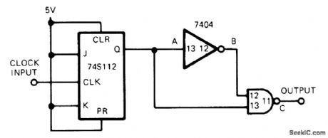
Developed for measuring impulse response of surface acoustic wave devices, for which pulse width had to be under 10 ns for frequency spectrum of about 100 MHz. Propagation delay time of 7404 inverter establishes output pulse width.-R. J. Lang, W. A. Porter, and B. Smilowitz, Simple Circuit Generates Nanosecond Pulses, EDN Magazine, Sept. 5, 1975, p 77-78. (View)
View full Circuit Diagram | Comments | Reading(826)
TEST_CODE_GENERATOR
Published:2009/7/15 1:53:00 Author:Jessie
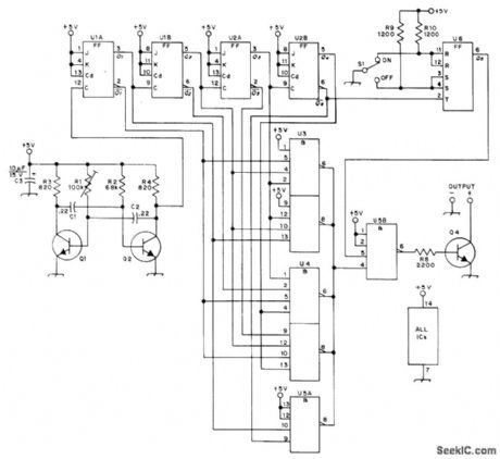
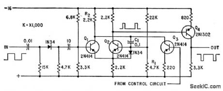
RTTY characters for R and Y are generated alternately in long series for checking system performance. (These letters give widest bandwidth of all character combinations.) Clock pulse at 45.5 Hz is generated by 2SC943 astable MVBR Q1-Q2. 74107 flip-flops U1A-U2B are connected as binary dividers for modulo-8 counter, so any bit between 0 and 7 is available for use with Signetics 8416A gates U3-U5 to feed desired character to 2SC372 output transistor. Automatic start/stop circuit using Fairchild 9945 docked flip-flop U6 ensures that sequence always starts with R and ends with Y. a4 conducts on mark and is cut off on space, for feeding frequency-shift keyer.-K. Sekine, A Simple RY Code Generator for TTY, QST, Dee. 1974, p 20-24. (View)
View full Circuit Diagram | Comments | Reading(1050)
QUADRATURE_OUTPUTS
Published:2009/7/15 1:52:00 Author:Jessie
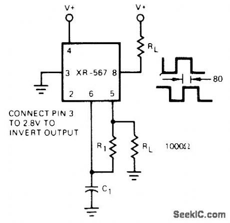
Exar XR-567 tone decoder is connected as precision oscillator providing separate square-wave outputs that are very nearly in quadrature phase. Typical phase shift between outputs is 80°. Supply voltage range is 5-9 V.- Phase-Locked Loop Data Book, Exar Integrated Systems, Sunnyvale, CA, 1978, p 41-48. (View)
View full Circuit Diagram | Comments | Reading(2329)
BAUDOT_TO_ASCII
Published:2009/7/15 1:51:00 Author:Jessie
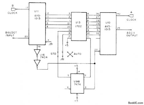
Used with Baudot RTTY codes on amateur bands, to drive Teletype ma chine requiring ASCII code. Separate 555 timers are used as clocks running at 727 Hz and at 1760 Hz. Provides only one-way conversion for receiving capability, but article gives companion circuit for two-way code conversion as required for transmission with ASCII Teletype. On U13, pins 12, 13, 15, 22, and 23 all go to +5 V along with pin 17; only pin 14 is grounded.-J. G. Mills, Baudot to ASCII Converter, 73 Magazine, Sept. 1977, p 80-85.
(View)
View full Circuit Diagram | Comments | Reading(1690)
554_ASTABLE
Published:2009/7/15 1:50:00 Author:Jessie
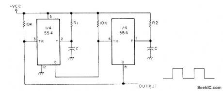
Two sections of 554 quad monostable timer are used. Output frequency is 1/ (R1 + R2) C hertz, and output duty cycle is 100R2/ (R1 + R2). When R1 is equal to R2, symmetrical square wave is obtained VCC is 4.5-16 V at 3-10mA.-H. M. Berlin, IC Timer Review, 73 Magazine,Jan. 1978, p 40-45.
(View)
View full Circuit Diagram | Comments | Reading(770)
KEYER_FOR_AFSK
Published:2009/7/15 1:48:00 Author:Jessie
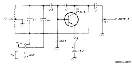
Uses one center-tapped 88-mH toroid tuned to desired RTTY space frequency by suitable value of C1 (0.0628μF for 2295 Hz). When relay is closed, suitable value for C2 (0.0156μF for 2125 Hz) is paralleled with C1 to give desired space frequency. Output is perfect sine wave. Plug output into audio input jack of transmitter. Plug relay coil directly into 150-V 60-mA loop of teleprinter. When loop current is turned on, relay closes and AFSK is on mark. Space frequency occurs when relay is opened by teleprinter keyboard.-J. B. Dillon, Audio-Frequency Shift Keyer, Ham Radio, Sept. 1976, p 45. (View)
View full Circuit Diagram | Comments | Reading(861)
TREBLE_BOOSTER_CIRCUIT
Published:2009/7/14 19:48:00 Author:May
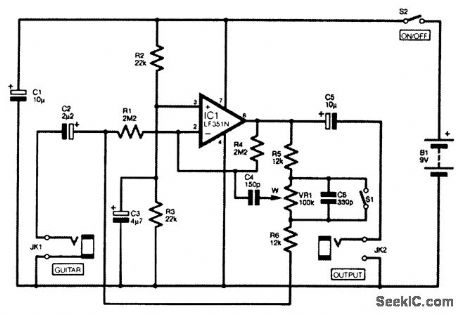
The circuit is basically a noninverting-mode amplifier. Resistors R2 and R3 bias IC1's noninverting input (pin 3), and R1 plus R4 act as a negative feedback network that sets the closed-loop volt-age gain of IC1 at unity. However, R1 and R4 are used only to set the operating conditions of IC1 at dc and at low to middle audio frequencies. The high-frequency voltage gain is governed by a more-complex negative feedback network that is composed of resistors R5 and R6, potentiometer VR1, and capacitors C4 and C6. R5, VR1, and R6 form a conventional negative feedback network that enables the voltage gain of the circuit to be varied. With the wiper (w) of VR1 toward the top end of its track, the circuit provides losses of nearly 20 dB. Moving the wiper down to the bottom gives almost 20 dB of gain. It is coupled to the inverting input via capacitor C4, which has quite a low value. Consequently, C4 provides an efficient coupling only at high frequencies. At middle and bass frequencies, capacitor C4 has a very high impedance and provides only a loose coupling to IC1's inverting input.Therefore, control VR1 is ineffective at these lower frequencies, where the voltage gain of the circuit is largely governed by resistors R1 and R4. This permits the required boost and cut to be obtained at high frequencies, but keeps the gain at about unity at middle and low (View)
View full Circuit Diagram | Comments | Reading(1377)
FSK_DECODER_1
Published:2009/7/15 1:46:00 Author:Jessie
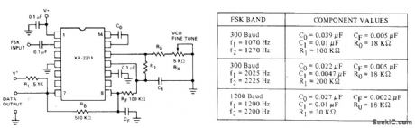
R0 and C0 set PLL center frequency for Exar XR-2211 FSK demodulator/tone decoder. R1 sets system bandwidth. C1 sets loop filter time constant and loop damping factor. CF and RF form postdetection filter for FSK data output. Table gives values for most commonly used FSK bands.- Phase-Locked Loop Data Book, Exar Integrated Systems, Sunnyvale, CA, 1978, p 29-34. (View)
View full Circuit Diagram | Comments | Reading(3502)
SCR_STATIC_ALTERNATOR
Published:2009/7/15 1:45:00 Author:Jessie
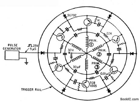
Silicon-controlled rectifiers serve as current-switching elements in ring-counter inverter that delivers three. phase ac output requiring no filtering, with .out moving parts. With 2.4-kc pulse genera tor, output is 400-cps three-phase.-R. H .Murphy, Developing True Solid-State Static Alternators, Electronics, 36:21, p 58-61. (View)
View full Circuit Diagram | Comments | Reading(1584)
ZENER_PROTECTS_METER
Published:2009/7/15 1:45:00 Author:Jessie
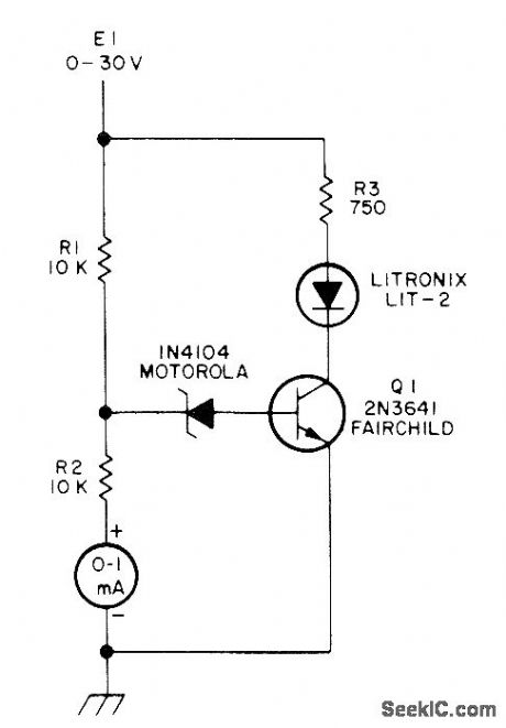
Simple overvoltage protection circuit makes 10-V zener conduct when voltage E1 being measured goes over 20-V full-scale limit of voltmeter using milliammeter movement with multiplier resistor R2. This turns on Q1, drawing current through LED to give visual indication of overvoltage, while providing protective shunt path around meter.-H. Olson, Sensitive Meters Saved, 73 Magazine, Oct. 1977, p 153. (View)
View full Circuit Diagram | Comments | Reading(952)
FSK_WITH_SLOPEAND_VOLTAGE_DETECTION
Published:2009/7/15 1:43:00 Author:Jessie
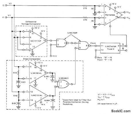
Motorola MC1545G gated video amplifier is used with slope and differential voltage comparators to provide switching of output alternately between input signal fl at 2975 Hz and f2 at 2125 Hz. With gate level on pin 1 of MC1545G high (greater than 1.5 V), signal applied between pins 4 and 5 is passed and signal between pins 2 and 3 is suppressed. With gate low (less than 0.5 V), situation is reversed. To avoid generation of spurious frequencies and noise, gate control voltage is allowed to change only when rate of change of fl and f2 have same sign and values of fl and f2 themselves have same sign and equal magnitude within several millivolts. Data rate is about 170 Hz.- Gated Video Amplifier Applications-the MC1545, Motorola, Phoenix, AZ, 1976, AN-491, p 12. (View)
View full Circuit Diagram | Comments | Reading(716)
PROGRAMMABLE_TIMER_SEQUENCER
Published:2009/7/14 19:40:00 Author:May
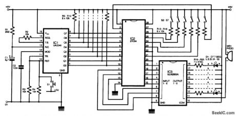
The circuit diagram of this programmable sequencer could be applied in a number of timing uses. Prior to the start of each interval, an audible tone is generated, and a seven-segment LED display shows the interval number. Prior to the end of that inerval, the buzzer sounds again. IC1 is a 2240 timer/counter device that clocks up to 256 periods, the durations of which are determined by resistor R1 and capacitor C1. The 2240 has its RESET and TRIGGER pins (10 and 11) wired via a push switch S1.The timer is used to operate a memory chip, IC2. The first 8 addressed bits are used by the timer/counter to step through the 256 steps available for each program. The other 6 bits are selected by an external switch network S2 to S7 which permits up to 26 programs, each of 256 steps. The 27C64 has eight outputs, which was enough for a single-digit LED display plus a piezo buzzer. (View)
View full Circuit Diagram | Comments | Reading(3160)
555_TIME_DELAY
Published:2009/7/14 19:38:00 Author:May
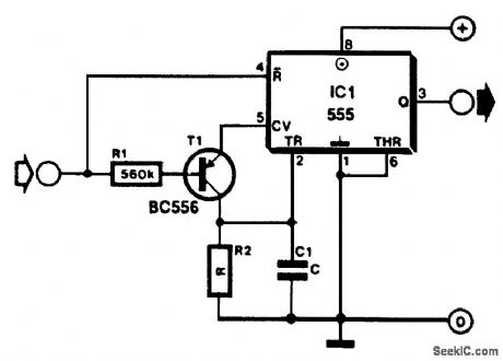
Many electronic circuits frequently require the brief delay of a pulse. Such a delay, here between 100μs and 100 seconds, is easily provided by a simple circuit based on the popular 555. That is more than adequate for most applications. The output of the 555 can go high only if the potential at pin 2 drops below a third of the level of the supply voltage, provided that the level at pin 4 is high. In quiescent operation, the level at pin 4 is low and C1 is charged via T1, so the output is low. When the input goes high, T1 is switched off and C1 is discharged via R1. In that condition, the REST state is cancelled and after a time delay that depends on the state of discharge of C1, the output of the 555 goes high .The time delay in seconds is calculated from r=0.69R1C1, where R1 must be greater than or equal to 10KΩ (View)
View full Circuit Diagram | Comments | Reading(3975)
400_CPS_THREE_PHASE_INVERTER_DELAY_CIR_CUIT
Published:2009/7/15 1:42:00 Author:Jessie
One-shot mvbr Q1-Q2 triggered by input signal, and Q3 controlled by error-detecting signals at output of static inverter, together determine delay at output of Q4.Complete inverter uses six identical delay circuits together with solid-state servo loops to control output voltages and phase angles despite unbalanced loads.-T. J. Gilliam, Three-Phase Inverter with Feedback Loops, Electronics, 35:12, p 48-5l. (View)
View full Circuit Diagram | Comments | Reading(769)
PLL_RTTY_TERMINAL
Published:2009/7/15 1:41:00 Author:Jessie

Uses 741 opamp as limiter, followed by NE565 phase-locked loop, another opamp U3 operating as voltage comparator or slicer, and keying transistor. Terminal requires no filters because incoming signal locks onto VCO whose frequency is placed between those of mark and space tones. As these tones alternate, output of PLL is made to pro-duce plus and minus voltages by connecting voltage comparator to output of NE565. Resulting plus voltage corresponds to mark tone and minus voltage to space tone for use in keying loop circuit of teleprinter. R1 is only adjustment required; article covers adjustment for receiver in SSB mode and in CW mode.-N. Stinnette, Phase-Locked Loop RTTY Terminal Unit, Ham Radio, Feb. 1975, p 36-37. (View)
View full Circuit Diagram | Comments | Reading(2558)
9600_CPS_AT_15_KW
Published:2009/7/15 1:37:00 Author:Jessie
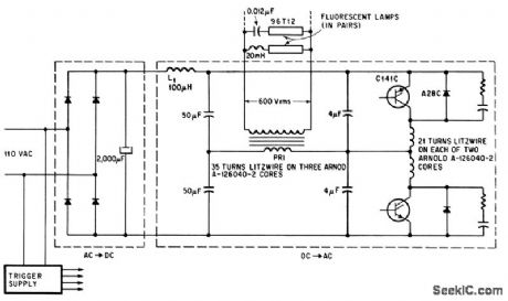
Scr inverter fluorescent lamps in parallel at 9,600 cps with power supply efficiency above 95%. Inverter operates safely without load during interval between turn. on and ionization. RC networks across diodes damp out ringing.-N. Mapham, SCR's Break the Frequency Barrier, Electronics, 38:18, p 88-97. (View)
View full Circuit Diagram | Comments | Reading(1498)
250_W_50_KC_INVERTER
Published:2009/7/15 1:35:00 Author:Jessie
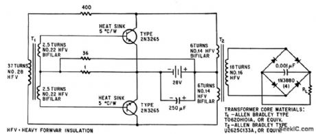
Silicon power transistors in high-speed inverter circuit give con version efficiency up to 90% in changing 28 v d-c to 50 kc at primary of output transformer.-H. T. Breece, Boosting D-C Voltage With Sillcon Transistors, Electronics, 37:29, p 56-66 (View)
View full Circuit Diagram | Comments | Reading(775)
| Pages:139/471 At 20121122123124125126127128129130131132133134135136137138139140Under 20 |
Circuit Categories
power supply circuit
Amplifier Circuit
Basic Circuit
LED and Light Circuit
Sensor Circuit
Signal Processing
Electrical Equipment Circuit
Control Circuit
Remote Control Circuit
A/D-D/A Converter Circuit
Audio Circuit
Measuring and Test Circuit
Communication Circuit
Computer-Related Circuit
555 Circuit
Automotive Circuit
Repairing Circuit