
Index 131
Quartz crystal sine wave oscillator circuit
Published:2011/8/7 1:42:00 Author:nelly | Keyword: Quartz crystal, sine wave, oscillator
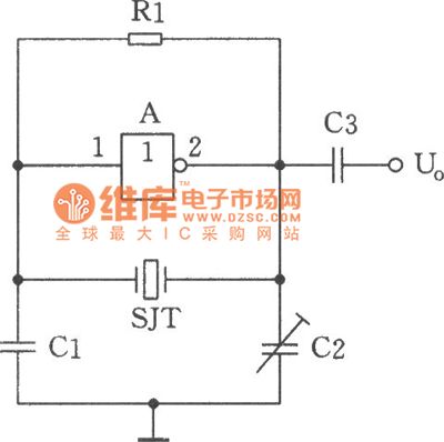
The picture shows the sine wave oscillator which is composed of the quartz crystal SJT and the gate A of the hex inverter IC CD4069.Compared with the ordinary RC phase-shift oscillator, the stability of crystal oscillator’s frequency can reach 10-5 or higher. This high index (The stability of the RC phase-shift oscillator’s frequency only can reach 10-2) can not be reached by the RC phase-shift oscillator. CMOS NAND gate and the negative feedback bias resistor R1 form the inverting amplifier circuit. Quartz crystal SJT, C1 and C1 form the 7c type positive feedback branch.
(View)
View full Circuit Diagram | Comments | Reading(2043)
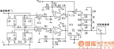
The wideband voltage controlled oscillator circuit composed of CD4046
Published:2011/8/6 2:35:00 Author:nelly | Keyword: wideband, voltage controlled, oscillator
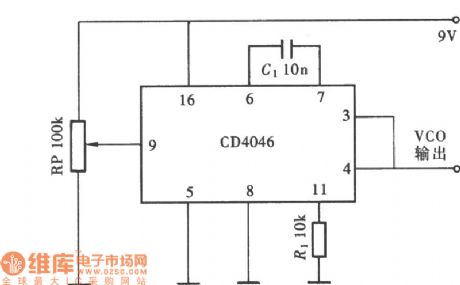
The wideband voltage controlled oscillator circuit composed of CD4046 is as shown: (View)
View full Circuit Diagram | Comments | Reading(4084)
The voltage controlled oscillator circuit composed of CD4007
Published:2011/8/6 2:44:00 Author:nelly | Keyword: voltage controlled, oscillator
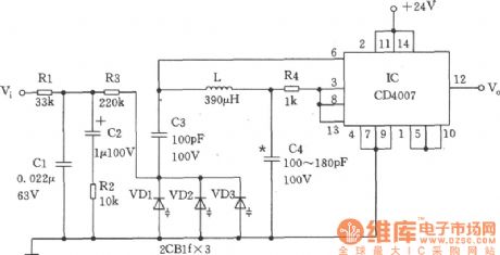
The voltage controlled oscillator is as shown. Through the low-pass filter Rl ~ R3, Cl~C2, this voltage controlled signal provides the varactor diode VDl ~ VD3 with DC voltage which will change with the frequency and phase. The output of the voltage controlled oscillator is composed of the inductor L, capacitor C3, C4 and varactor diode VDl ~ VD3 and integrated circuit IC (CD4007). (View)
View full Circuit Diagram | Comments | Reading(3413)
CMOS gate voltage-controlled oscillator circuit
Published:2011/8/6 3:26:00 Author:nelly | Keyword: CMOS, gate, voltage-controlled, oscillator
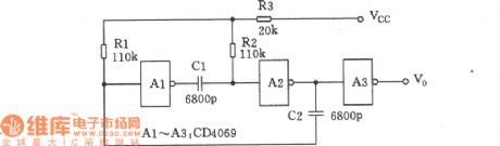
As it is shown in the figure, two non-gates A1 and A2 form the self-excited multivibrator. The oscillation frequency of the circuit will change with the size of the control voltage. When the value of Vcc is closed to the threshold, its influence to RC’s charge and discharge is the smallest, so the oscillation will be the lowest. When the Vcc is far from the threshold, the discharge and charge of the capacitor will be faster, so the oscillation will be higher.
(View)
View full Circuit Diagram | Comments | Reading(747)
Fast and synchronized voltage-controlled oscillator circuit
Published:2011/8/6 21:16:00 Author:nelly | Keyword: Fast, synchronized, voltage-controlled oscillator
This circuit is mainly used to connect the phase splitter and analog converter together, so the high-stable voltage-controlled oscillator and the external reference frequency can be synchronized precisely.
(View)
View full Circuit Diagram | Comments | Reading(688)
Voltage-controlled duty cycle oscillator circuit
Published:2011/8/7 4:14:00 Author:nelly | Keyword: Voltage-controlled, duty cycle, oscillator
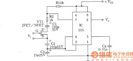
The picture shows the self-excited multivibrator which is composed of 555 timer. FET VTl is used as the voltage-controlled resistor (VVR). Changing the voltage gate source VGS can alter the resistor between JEFT drain (D) and source (S). Two coupling capacitors can avoid the DC voltage of circuit’s other part from influencing VTl. In order not to make the coupling capacitor influence the charging and discharging time of 555 timer. The values of coupling capacitor C1 and C2 are ten times of timing capacitor, meanwhile, a resistance RDS can be achieved between the D pole and S pole of VTl.
(View)
View full Circuit Diagram | Comments | Reading(1629)
Exponential voltage-controlled oscillator (555) circuit
Published:2011/8/6 3:14:00 Author:nelly | Keyword: Exponential, voltage-controlled, oscillator
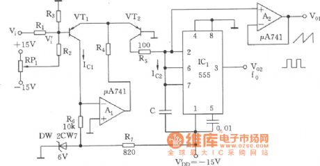

The relationship of Vi~555 oscillator frequency fo:
(View)
View full Circuit Diagram | Comments | Reading(1629)
The voltage-controlled oscillator circuit with triangular and square wave output
Published:2011/8/6 21:43:00 Author:nelly | Keyword: voltage-controlled, oscillator, triangular wave, square wave
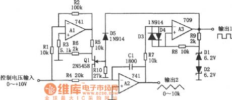
The figure shows the voltage-controlled oscillator circuit with triangular and square wave output. This circuit is the oscillator controlled by the voltage. It has the good stability and excellent linearity, and it also has the wide frequency range. This circuit has two output ends, one is the square wave output end, and the other is the triangle wave output end. In the picture, A1 is the inverter; A2 is the integrator; A3 is the comparator. FET Q1 is used to change the direction of integration. The reference voltage of the comparator is provided by the zener diode D1 and D2. (View)
View full Circuit Diagram | Comments | Reading(871)
The pulse generator circuit composed of CD4011
Published:2011/8/6 21:24:00 Author:nelly | Keyword: pulse generator
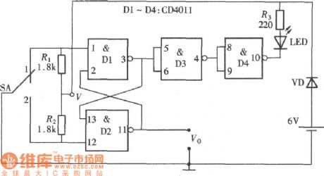
As shown in the picture, the logic pulse generator can transmit the negative or positive logic pulse, according to the need. This circuit is composed of a four-two input end and the non gate CD4011, among which D1 and D2 form a RS trigger pulse, and D3 and D4 are used as the inverters. It will be isolated with the D1 output end and drive a LED, thus the logic state of the output pulse can be indicated. (View)
View full Circuit Diagram | Comments | Reading(1660)
The pulse and pulse train generator circuit composed of CD4093
Published:2011/8/7 4:21:00 Author:nelly | Keyword: pulse, pulse train, generator
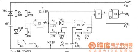
The pulse and pulse train generator is mainly composed of a four - two input Schmitt trigger CD4093 and a button switch. When the button is pressed, the circuit will output a single pulse. When the button is pressed for a period of time, the circuit will output the pulse train. The composition of the circuit is as shown in the picture. This circuit is composed of the button switch, input control circuit, pulse oscillator and pulse output circuit.
(View)
View full Circuit Diagram | Comments | Reading(2711)
VIDEO_INVERTER
Published:2009/7/14 21:42:00 Author:May
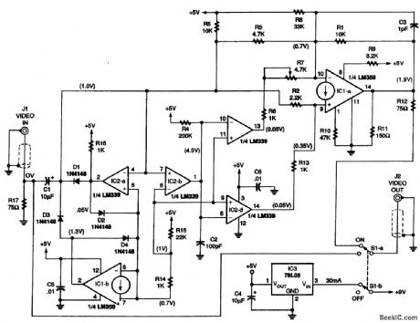
This video inverter circuit is based on an LM359 dual Norton op amp and an LM339 quad voltage comparator for dc restoration, sync detection and processing, and buffering and inversion of the video signal. The dc level of the video signal is restored to 0.7 V because the inputs of IC1-b operate at one diode voltage drop above ground. Comparator IC2-b acts as a threshold detector set to detect sync pulses 300 mV above the restored dc level of 0.7 V. Components C2 and R4 stretch the detected 4-μs sync pulses to 8μs to include the duration of 8 cycles of 3.58-MHz color burst after the input sync pulse. Comparators IC2-c and IC2-d buffer the stretched sync pulse with open-collector out-puts at pin 13 and 14 to gate the buffer/inverter action of the main amplifier IC1-a. Resistor R3 sets the gain of the inverting input of the main video amplifier IC1-a to 2 (-R1/R3= -2), and R4 sets the gain of the noninverting input of IC1-a to 4 (R1/R4=+4) These two inputs combine to achieve an overall gain of +2 as a buffer or -2 as an inverter. During the sync and color-burst portions of the in-put signal, the IC2-c and IC2-d outputs are open and the overall gain is +2. The rest of the time, a low at the output of IC2-d (pin 14) short-circuits the noninverting +4 signal path for an overall gain of -2, while a low at lC2-c pin 13 injects the necessary offset in the inverted video signal to keep it above the black level. Potentiometer R7 adjusts the black level at the output to correspond to the peak white level in the negative. Resistor R12 matches the output for 75Ω. A 78L05 regulator (IC3) provides a stable 5-V supply from a 9-V battery or ac adapter. (View)
View full Circuit Diagram | Comments | Reading(3495)
PULSE_FREQUENCY_DIVIDER_1
Published:2009/7/14 21:42:00 Author:May
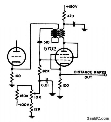
Plate-to-grid coupled blocking oscillator, with voltage step-up to grid, is used to divide from high to low pulse frequency.-NBS, Handbook Preferred Circuits Navy Aeronautical Electronic Equipment, Vol. 1, Electron Tube Circuits, 1963, p N7-1. (View)
View full Circuit Diagram | Comments | Reading(1011)
PHANTASIRON_FREQUENCY_DIVIDER
Published:2009/7/14 21:40:00 Author:May
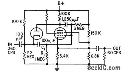
Will divide 360 cps to give 60 cps. Is triggered by pulse train with hoth positive and negative pulses.-K. M. Chen, Trigger Stabilizes Frequency Divider, Electronics, 31:47, p 104-107. (View)
View full Circuit Diagram | Comments | Reading(814)
VARIABLE_TURN_ON_AND_TURN_OFF
Published:2009/7/14 21:40:00 Author:May
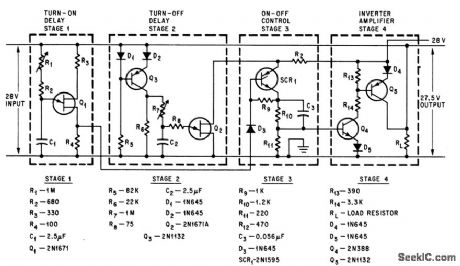
Both input and output delays are variable from 1.5 to 1,500 millisec. Maximum turn-on delay cannot exceed duration of input pulse. -C. R. Mora, Delay Circuit Varies Turn-on, Turn-off, Electronics, 39:7, p 92-93. (View)
View full Circuit Diagram | Comments | Reading(892)
PULSE_FREQUENCY_DIVIDER_2
Published:2009/7/14 21:45:00 Author:Jessie
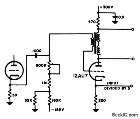
Plate-to-grid coupled blocking oscillator, with voltage step-down to grid, is used to divide from high to low pulse frequency. Stepdown yields maximum peak pulse voltage at plate and per mits maximum pulse duration from given transformer.-NBS, Handbook Preferred Circuits Navy Aeronautical Electronic Equipment, Vol. 1, Electron Tube Circuits, 1963, p N7-1. (View)
View full Circuit Diagram | Comments | Reading(943)
DIVIDER_ELIMINATES_COUNT_STARTING_JITTER
Published:2009/7/14 21:45:00 Author:Jessie
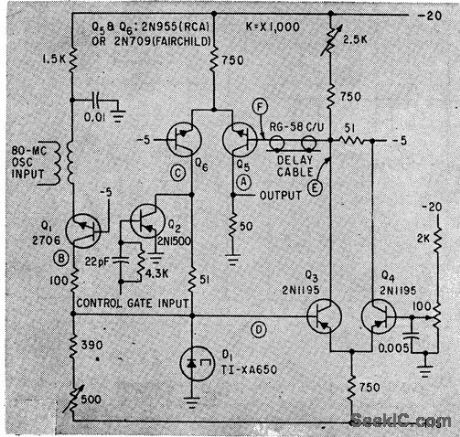
Output of 80-Mc free-running crystal oscillator is divided by 8 to give 10-Mc time base that is almost perfect square wave.-W.O. LeCroy, Jr., Eliminating One-Count Uncertainty in Cycle-Counting Interval Timers, Electronics, 35:29, p 46-47. (View)
View full Circuit Diagram | Comments | Reading(729)
SIMPLE_ALL_PASS_FILTER
Published:2009/7/14 21:53:00 Author:Jessie
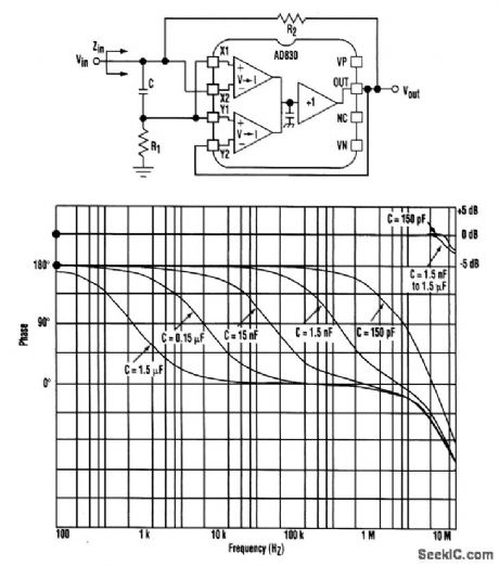
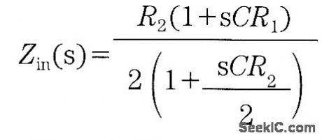
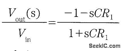
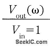
A very simple all-pass implementation can be realized with an active-feedback amplifier like the AD830 or the LTC1193. R1 and C set the filter’s actual transfer function, while R2 is needed to provide a purely real input impedance over the frequency range of the AD830 (necessary for measurement reasons). The filter’s two basic equations are and from which we can see that the magnitude is constant:and the phase of Vout/Vin as a function of ω is 180°-2 tan-1 (ωCR1)From the first equation, it's clear that for Zin to be purely real, R1 has to be equal to R2/2, which implies Zin=R1. Once C is chosen, R1 and R2 can be picked according to the termination and required phase shift. The graph shows the circuit's performance for Vs=±15V, R1=100,R2=200, and values of C from 1.5 μF to 150 pF with 90° phase shifts at one-decade increments up to 10 MHz.
(View)
View full Circuit Diagram | Comments | Reading(1072)
BUFFERED_PEAK_DETECTOR
Published:2009/7/14 21:52:00 Author:Jessie
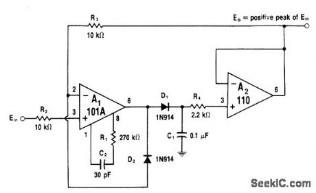
Discharge current through C1 minimized by using low-input-current voltage follower A2. R3 allows A1 to be clamped in OFF state by D2 to give faster recovery. Circuit operates much like ideal diode, but with C1 storing DC voltage equal to peak input voltage value. When input signal crosses zero, A1 drives D1 on and circuit output follows rising signal slope. When input signal reaches peak and reverses, C1 is left charged. Reverse diode connections to detect negative peaks. Value of R1 should be increased to 2.7 megohms if C1 is increased to 1μF to improve stability.-W. G. Jung, IC Op-Amp Cookbook, Howard W. Sams, Indianapolis, IN, 1974, p 196-197. (View)
View full Circuit Diagram | Comments | Reading(819)
TEMPERATURE_COMPENSATED_CURRENT_SOURCE1
Published:2009/7/14 21:50:00 Author:Jessie
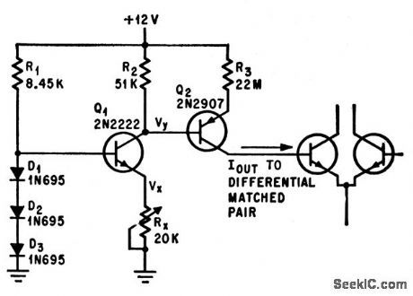
Presents 1,000 meg of output impedance while supplying up to 200 na of temperature-compensated current. Germanium diodes serve as compensating network drawing 1.3 ma. Based on fact that matched transistor pairs have base-current temperature coefficients that are predictable as function of operating current-C. C. Hanson, Low. Drift Current Generator Compensates for Temperature, Electronics, 39:12, p 108-109. (View)
View full Circuit Diagram | Comments | Reading(755)
RING_DETECTOR
Published:2009/7/14 21:54:00 Author:Jessie
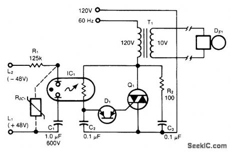
Optoisolator using neon lamp and light-dependent resistor serves as interface between telephone line and line-operated remote bell. Neon fires reliably from nominal 100-VAC ring signal, while capacitor C1 provides isolation required to prevent latch-up by sustaining voltages within range of phone-line quiet battery. If optional protective varistor RIC1 is added, rating of capacitor can be reduced to 400 V. Triac Q1 in series with primary of line transformer provides synchronization to 20-Hz ringing frequency of phone system.-W. D. Kraengel, Jr. Ring Detector Optically Interfaces Phone, EDN Magazine, Aug. 5.1978, p 80 and 82. (View)
View full Circuit Diagram | Comments | Reading(2348)
| Pages:131/471 At 20121122123124125126127128129130131132133134135136137138139140Under 20 |
Circuit Categories
power supply circuit
Amplifier Circuit
Basic Circuit
LED and Light Circuit
Sensor Circuit
Signal Processing
Electrical Equipment Circuit
Control Circuit
Remote Control Circuit
A/D-D/A Converter Circuit
Audio Circuit
Measuring and Test Circuit
Communication Circuit
Computer-Related Circuit
555 Circuit
Automotive Circuit
Repairing Circuit