
Basic Circuit
Index 3
MT-700 voice Phychopsis circuit diagram
Published:2014/4/14 22:01:00 Author:lynne | Keyword: MT-700 voice Phychopsis circuit diagram
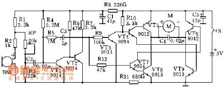
Voice UFO is a mechatronic device, which includes an electronic control circuit and mechanical operation of the device of two parts, mechanical parts working condition is controlled by an electronic circuit. Using voice and delay steering control DC motor control circuit. Circuit includes a total of three parts, from left to right: the sound signal receiving circuit electret microphone BM, etc.; transistor VT1, VT2 and R5, C3, etc. The delay control circuit; transistor VT3 ~ VT9 like the a motor drive circuit.
When no sound signal, delay control circuit of two transistors VT1 end, VT2 conduction, output low, through the VT3, VT4, VT7, ultimately complementary driver transistor VT5, VT9 conduction, VT6, VT8 off, the motor M Forward, Voice UFO straight forward. R5, C3 is connected across the output of the delay control circuit (VT2 collector) to the input terminal (VT1 base), so that C3 is fully charged (the left and right being negative). When receiving the BM electret microphone sound signal, and outputs a positive pulse is coupled to the delay control circuit C2, VT1 conduction, VT2 off, the output from low to high, so that the drive tube VT5, VT9 off, VT6, VT8 conduction, motor M reversal, Voice UFO backwards. Voice UFO front wheel bracket designed as a special structure, making the front wheels automatically when reverse deflection angle, so voice flying saucer at the same time that their own turn backwards. Because of the delay before the network R5, C3 exists, the sound signal disappears, the delay control circuit outputs remain high for a few seconds, Voice UFO turned backwards a few seconds to recover straight forward.
The main components and structural parts Some of the major components of electronic circuits, including: 9012-type PNP transistor, NPN transistor type 9013, 9014 type NPN transistor, electret microphone, capacitors, electrolytic capacitors, resistors, trimming potentiometers, power switch, and a printed circuit board, battery box, DC motors. The mechanical part of the main structure are: Body panels, tail panels, front wheel and front wheel bracket, rear and rear bracket, motor bracket, reduction gear set, transparent top cover and screws, nuts and so on. Debugging Mainly to adjust the voice sensitivity: the Voice UFO in the hand, mounted on two AA batteries, turn the power switch S, then UFO rear wheel should forward. Issue a voice password, and adjust trimmer potentiometer RP, so that voice sensitivity is moderate, UFO rear reliably can be reversed with a password. (View)
View full Circuit Diagram | Comments | Reading(1533)
ND-0 Mounting Bracket Diagram
Published:2014/4/14 22:08:00 Author:lynne | Keyword: ND-0 Mounting Bracket Diagram

To facilitate the ND series when vibration sensing circuit to control the installation and use, especially for the design of ND-0 mounting bracket, it can give full play to the performance of the sensor, and simplifies installation difficulty, its shape and the holes shown in Figure, using the sensor 914 ND epoxy glue or bracket fixed on the plane, the two holes for the other side of the body to be detected together.
(View)
View full Circuit Diagram | Comments | Reading(1314)
Use half adder and full adder of four additive operation circuit diagram
Published:2014/4/13 21:00:00 Author:lynne | Keyword: Use half adder and full adder of four additive operation circuit diagram
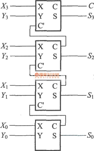
Use half adder and full adder of four additive operation circuit diagram shown as follow:
(View)
View full Circuit Diagram | Comments | Reading(1356)
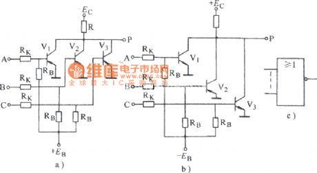
Full adder circuit diagram
Published:2014/4/13 21:03:00 Author:lynne | Keyword: Full adder circuit diagram
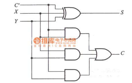
Full adder circuit diagram as shown:
(View)
View full Circuit Diagram | Comments | Reading(1605)
The mechanical part of electronic circuitry circuit diagram
Published:2014/4/13 21:33:00 Author:lynne | Keyword: The mechanical part of electronic circuitry circuit diagram
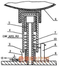
Electronic scale mechanical parts, as shown in the fixed on metal substrate 1 a guide pillar 2, position the club set on pillar 3, bushing bearing spring 7, and in the spring pressing sleeve cover on 5, on the pressing sleeve combined with a 4 cylinder, the plastic container liners placed with the base plate of 6. Sliding resistor in the bridge 8 (RP2) measured in turn 1, 9 on the base of the RP2 arm into the removable barrel hole. The height of the structure is associated with the sliding resistor of spring rigidity and selection, selection of spring principle is: when the maximum measured object weight, a spring compression relative sliding resistor RP2 slider stroke length of around 50-6 d %. To connect power supply automatically when measuring weight, on the base plate fixed a use electromagnetic relay contact reformed from a spring leaf slice of 10, and the distance between the protection of Jane for 0.5 LMM.
Electronic circuits of electronic parts, except the sliding potentiometer RP Sally and indicating meter PAl, installed on the diagram shown in printed circuit board.
(View)
View full Circuit Diagram | Comments | Reading(1438)
Half adder circuit diagram
Published:2014/4/10 22:09:00 Author:lynne | Keyword: Half adder circuit diagram
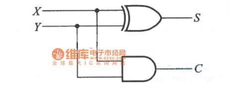
Half adder circuit diagram shown as follow:
Value table:
(View)
View full Circuit Diagram | Comments | Reading(1383)
Transistor NOR gate circuit diagram
Published:2014/4/10 21:47:00 Author:lynne | Keyword: Transistor NOR gate circuit diagram
Transistor NOR gate circuit diagram as shown:
(View)
View full Circuit Diagram | Comments | Reading(1558)
Transistor or gate circuit diagram
Published:2014/4/10 21:43:00 Author:lynne | Keyword: Transistor or gate circuit diagram
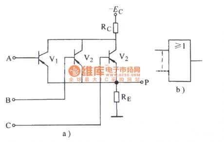
Transistor or gate circuit diagram shown as follow:
(View)
View full Circuit Diagram | Comments | Reading(1395)
Two-input NOR gate resistance of a transistor circuit diagram
Published:2014/4/10 21:42:00 Author:lynne | Keyword: Two-input NOR gate resistance of a transistor circuit diagram
Two-input NOR gate resistance of a transistor circuit diagram as shown:
(View)
View full Circuit Diagram | Comments | Reading(1314)
Resistance-transistor gate circuit diagram
Published:2014/4/10 21:41:00 Author:lynne | Keyword: Resistance-transistor gate circuit diagram
Resistance - transistor gate circuit diagram shown as follow:
(View)
View full Circuit Diagram | Comments | Reading(1419)
Two input transistor nand gate circuit diagram
Published:2014/4/9 21:20:00 Author:lynne | Keyword: Two input transistor nand gate circuit diagram
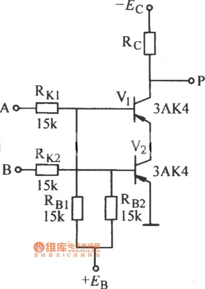
Two input transistor nand gate circuit diagram as shown:
(View)
View full Circuit Diagram | Comments | Reading(1592)
Two input transistor nor gate circuit diagram
Published:2014/4/9 21:20:00 Author:lynne | Keyword: Two input transistor nor gate circuit diagram
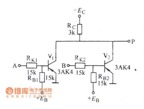
Two input transistor nor gate circuit diagram shown as follow:
(View)
View full Circuit Diagram | Comments | Reading(1619)
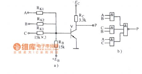
Diode and gate decoding circuit (two) Schematic
Published:2014/4/9 21:19:00 Author:lynne | Keyword: Diode and gate decoding circuit (two) Schematic
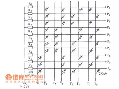
Diode and gate decoding circuit (two) Schematic shown as follow:
(View)
View full Circuit Diagram | Comments | Reading(1476)
Diode and gate decoding circuit (one) Schematic
Published:2014/4/9 21:14:00 Author:lynne | Keyword: Diode and gate decoding circuit (one) Schematic
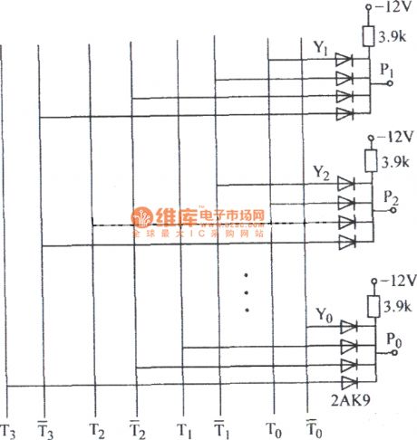
Diode and gate decoding circuit (one) Schematic shown as follow:
(View)
View full Circuit Diagram | Comments | Reading(1407)
Promote grounding load large current negation gate circuit diagram
Published:2014/4/8 21:13:00 Author:lynne | Keyword: Promote grounding load large current negation gate circuit diagram
Promote grounding load large current negation gate circuit diagram shown as follow:
(View)
View full Circuit Diagram | Comments | Reading(1424)
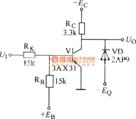
Zener diode clamping of the gate circuit diagram
Published:2014/4/8 21:07:00 Author:lynne | Keyword: Zener diode clamping of the gate circuit diagram
Zener diode clamping of the gate circuit diagram as shown:
(View)
View full Circuit Diagram | Comments | Reading(1431)
Output has a clamp diode gate circuit diagram
Published:2014/4/8 21:01:00 Author:lynne | Keyword: Output has a clamp diode gate circuit diagram
Output has a clamp diode gate circuit diagram shown as follow:
(View)
View full Circuit Diagram | Comments | Reading(1291)
Threshold NAND gate with a front level gate resistance circuit diagram
Published:2014/4/8 20:53:00 Author:lynne | Keyword: Threshold NAND gate with a front level gate resistance circuit diagram
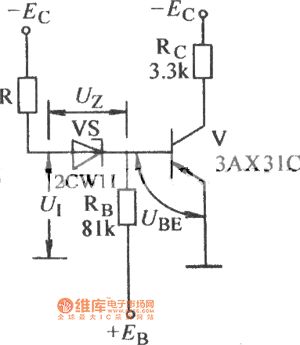
Threshold NAND gate with a front level gate resistance circuit diagram shown as follow:
(View)
View full Circuit Diagram | Comments | Reading(1483)
Sail power sunroof circuit diagram
Published:2014/4/7 21:31:00 Author:lynne | Keyword: Sail power sunroof circuit diagram
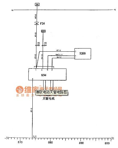
Sail power sunroof circuit diagram shown as follow:
(View)
View full Circuit Diagram | Comments | Reading(1442)
FM receiver circuit diagram
Published:2014/4/3 20:45:00 Author:lynne | Keyword: FM receiver circuit diagram
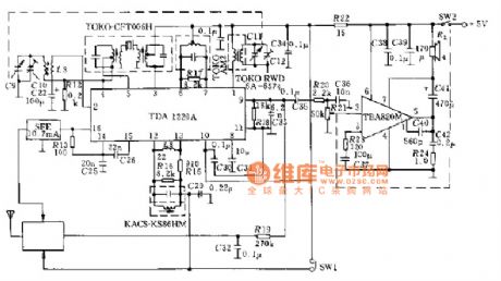
FM receiver circuit diagram shown as follow:
(View)
View full Circuit Diagram | Comments | Reading(1875)
| Pages:3/471 1234567891011121314151617181920Under 20 |
Circuit Categories
power supply circuit
Amplifier Circuit
Basic Circuit
LED and Light Circuit
Sensor Circuit
Signal Processing
Electrical Equipment Circuit
Control Circuit
Remote Control Circuit
A/D-D/A Converter Circuit
Audio Circuit
Measuring and Test Circuit
Communication Circuit
Computer-Related Circuit
555 Circuit
Automotive Circuit
Repairing Circuit