
Basic Circuit
Index 4
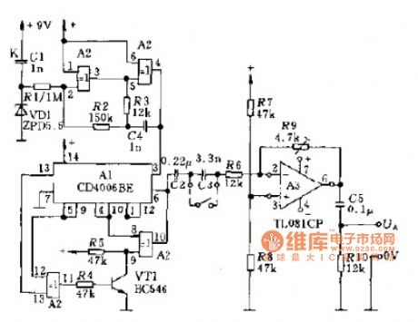
Sail anti-theft system circuit diagram
Published:2014/4/3 20:38:00 Author:lynne | Keyword: Sail anti-theft system circuit diagram
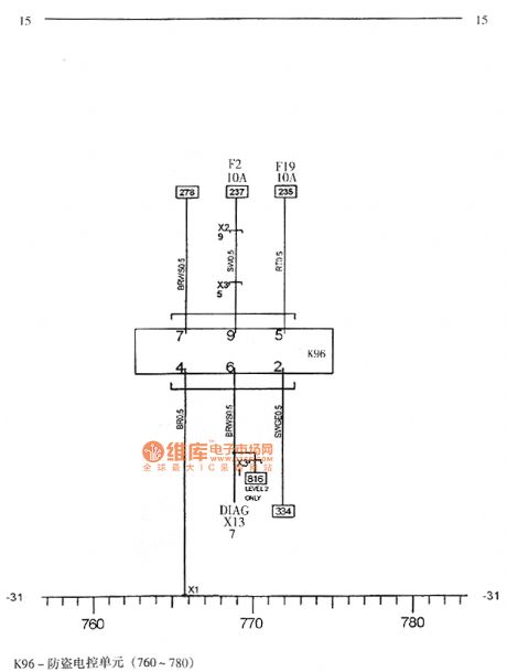
Sail anti-theft system circuit diagram shown as follow:
(View)
View full Circuit Diagram | Comments | Reading(1357)
Sail airbag system schematic
Published:2014/4/2 21:18:00 Author:lynne | Keyword: Sail airbag system schematic
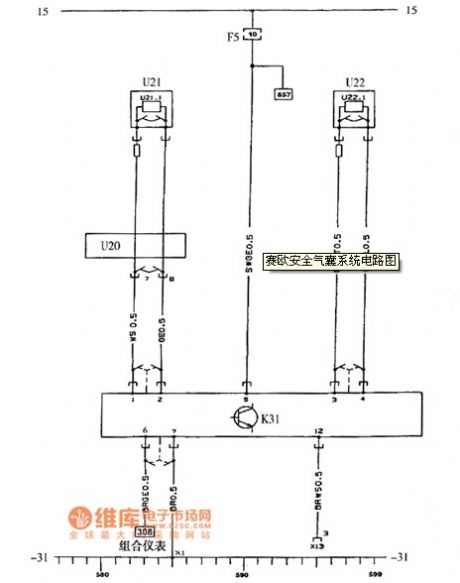
Sail airbag system schematic as shown:
(View)
View full Circuit Diagram | Comments | Reading(1428)
F-V conversion circuit schematic
Published:2014/4/2 21:12:00 Author:lynne | Keyword: F-V conversion circuit schematic

F-V conversion circuit schematic shown as follow:
(View)
View full Circuit Diagram | Comments | Reading(1701)
The LM35D interface circuit diagram
Published:2014/4/2 21:09:00 Author:lynne | Keyword: The LM35D interface circuit diagram,
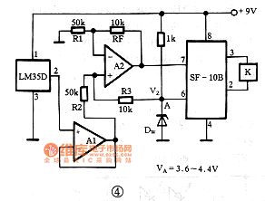
The interface circuit LM35D LM35D sensitivity of 10mV / ℃, it is up to 1V at 100 ℃ output. As the SF-10 instrument amplifier maximum input voltage of 240mV, so the higher the maximum temperature of the output signal LM35D to be attenuated. Further, LM35D voltage signal is output to ground, it can not directly access the output signal of the two inputs of the SF-10B (the ground pin ⑥, a single power amplifier device can not work), which requires the output voltage decays , and after the transfer circuit voltage to the interface with the SF-10B, as shown in FIG.
(View)
View full Circuit Diagram | Comments | Reading(1585)
Telecom filter circuit schematic
Published:2014/4/2 21:20:00 Author:lynne | Keyword: Telecom filter circuit schematic
Telecom filter circuit schematic shown as follow:
(View)
View full Circuit Diagram | Comments | Reading(1501)
A voice control recording circuit diagram
Published:2014/4/1 21:26:00 Author:lynne | Keyword: A voice control recording circuit diagram
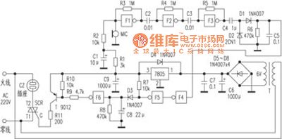
When a sound wave compression electret microphone MIC, MIC can output a weak audio signal fed from the NAND gate F1, F2, F3 and R3, R4, R5 constitute the three continuous linear amplification of the amplifier circuit , if consider peak waveform distortion , the output signal amplitude F3 has been large enough , after this signal is coupled through C4 by D1, D2 rectifier get unipolar pulses C5 charging. VC5 soon more than 1/2VDD, the output of NAND gate F4 0, F5 output is 1 , high charge to C8, VC8 also soon be greater than 1/2VDD, F6 output is 0 , the transistor T saturated conduction , SCR is trigger , so 220V mains supply via socket CZ to the recorder , recording starts ; If the sound disappears, the C5 voltage can not be maintained , VC5 quickly dropped to zero. Similarly , C8 only slowly discharge to R8, VC8 about three seconds after the drop to 0 , then , SCR deadline , tape recorders recording aborted ; so, automatic recording control recording ( if necessary delay longer available appropriate to increase the capacity of C8 ) .
This control circuit is not only used for automatic recording recorder can also be extended to other appliances require intermittent voice, interested friends can do it. If the sensitivity is not satisfied, it can be in F1 before adding a transistor amplifier.
(View)
View full Circuit Diagram | Comments | Reading(1740)
Signal repeater circuit diagram
Published:2014/4/1 21:16:00 Author:lynne | Keyword: Signal repeater circuit diagram
Signal repeater circuit diagram as shown:
(View)
View full Circuit Diagram | Comments | Reading(2382)
Transmission of data coupling circuit diagram
Published:2014/3/31 21:27:00 Author:lynne | Keyword: Transmission of data coupling circuit diagram
Transmission of data coupling circuit diagram shown as follow:
(View)
View full Circuit Diagram | Comments | Reading(1443)
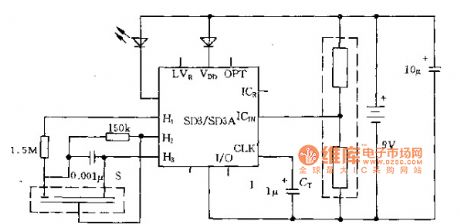
FAW Hongqi buzzer system schematics
Published:2014/3/31 21:30:00 Author:lynne | Keyword: FAW Hongqi buzzer system schematics
FAW Hongqi buzzer system schematic as shown:
(View)
View full Circuit Diagram | Comments | Reading(1368)
Noise generator circuit schematics
Published:2014/3/30 21:30:00 Author:lynne | Keyword: Noise generator circuit schematics
Noise generator circuit schematics shown as follow:
(View)
View full Circuit Diagram | Comments | Reading(1806)
Speech filter circuit diagram
Published:2014/3/30 21:24:00 Author:lynne | Keyword: Speech filter circuit diagram
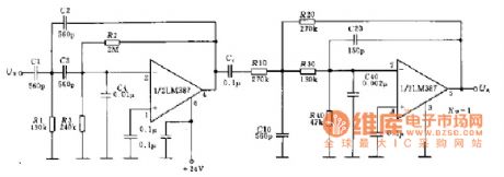
Speech filter circuit diagram as shown:
(View)
View full Circuit Diagram | Comments | Reading(1997)
Signal generator circuit diagram
Published:2014/3/30 21:21:00 Author:lynne | Keyword: Signal generator circuit diagram
Signal generator circuit diagram as shown:
(View)
View full Circuit Diagram | Comments | Reading(1387)
Eight AD7416 parallel circuit diagram
Published:2014/3/26 21:43:00 Author:lynne | Keyword: Eight AD7416 parallel circuit diagram, AD7416
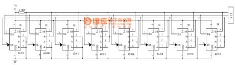
D7416 serial address low 3 can be set by the user, allowing a choice from 1001000 to 1001111 of eight addresses. 8 illustrates the AD7416 has received a serial bus system, their OTI output line to form a common interrupt request lines.
(View)
View full Circuit Diagram | Comments | Reading(1523)
Hardware schematic circuit
Published:2014/3/26 21:41:00 Author:lynne | Keyword: Hardware schematic circuit
Hardware schematic is shown in Figure. This is an evaluation circuit, which can install three digital temperature sensor: AD7414, AD7416, AD7814, the software displays each device in turn measured ambient temperature and OTI analog outputs with LED indication. Some explanations are now as follows:
(1) address of each device is different, and SDA, DOUT leads can be connected directly; AD7414, OTI output line (active low), now overrun alarm indication for the AD7416. (2) due to the inertia of the temperature coefficient of the larger, can be a simple and effective method of moving average, median method, low-pass filtering method for software filtering. In practical applications, the side of the sample side, the average of the average value as the temperature samples. Sampling frequency of 8 to 16 times can be. (3) The system uses LCM103 LCD module for temperature display, X25045 for power-on reset and watchdog with. (View)
View full Circuit Diagram | Comments | Reading(1642)
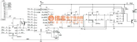
Four packages of AS300 circuit board
Published:2014/3/25 21:38:00 Author:lynne | Keyword: Four packages of AS300 circuit board, AS300
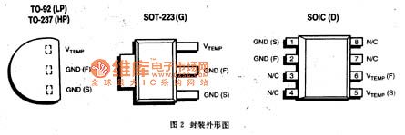
AS300 four packages shown (top view), each pin functions:
GND (S) selectable detection feet ground, and the substrate GND GND (F) is not connected. GND (F): signal ground and the circuit substrate grounding pin. VTEMP (F): output pin. The pin voltage is proportional to temperature. When 27 ℃, VTEMP = 3V, VTEMP with increasing temperature at a rate of 10mV / ℃ increases. VTEMP (S): selectable sensor VTEMP the output, use only on 8LSOIC package. (View)
View full Circuit Diagram | Comments | Reading(1396)
Digital pressure gauge based on MPX2100 circuit diagram
Published:2014/3/25 21:34:00 Author:lynne | Keyword: Digital pressure gauge based on MPX2100 circuit diagram, MPX2100
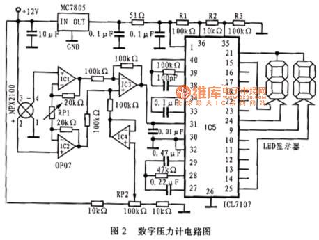
Digital pressure gauge based MPX2100 Digital pressure gauge MPX2100 configured as shown. MPX2100 operating voltage of 12V, the pressure between the sensor signal output 4 feet and 2 feet to IC1, IC2 amplification, amplifier gain is 1 +40 / RP1, IC1, IC2 connected to non-inverting input impedance state, the instrument can be obtained required high input impedance amplifier; IC3 is a unity gain differential amplifier, which can achieve high CMRR, IC4 and RP2 voltage divider circuit zeroing circuitry, RP1 used to adjust the gain of the amplifier circuit to complete the full digital display of pressure calibration range. IC3 output voltage to the A / D converter analog input voltage terminal IC5 (31 feet), the digital conversion by IC5 to drive LED display size of the pressure.
(View)
View full Circuit Diagram | Comments | Reading(3302)
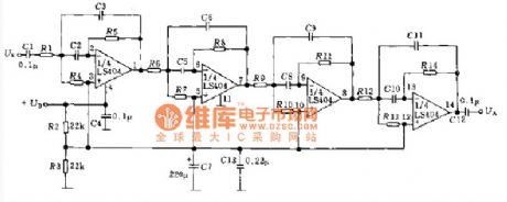
Multiple feedback type second-order bypass filter circuit diagram
Published:2014/3/24 21:26:00 Author:lynne | Keyword: Multiple feedback type second-order bypass filter circuit diagram
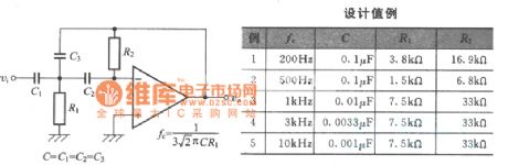
Multiple feedback type second-order bypass filter circuit diagram shown as follow:
(View)
View full Circuit Diagram | Comments | Reading(1619)
Differential circuit diagram
Published:2014/3/23 21:35:00 Author:lynne | Keyword: Differential circuit diagram
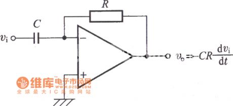
Differential circuit diagram as shown:
(View)
View full Circuit Diagram | Comments | Reading(1315)
The first-order bypass filter circuit diagram
Published:2014/3/23 21:34:00 Author:lynne | Keyword: The first-order bypass filter circuit diagram

The first-order bypass filter circuit diagram shown as follow:
(View)
View full Circuit Diagram | Comments | Reading(1760)
Add operation circuit diagram
Published:2014/3/23 21:33:00 Author:lynne | Keyword: Add operation circuit diagram
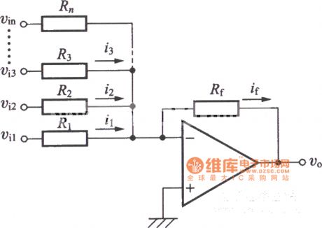
Add operation circuit diagram as shown:
(View)
View full Circuit Diagram | Comments | Reading(1468)
| Pages:4/471 1234567891011121314151617181920Under 20 |
Circuit Categories
power supply circuit
Amplifier Circuit
Basic Circuit
LED and Light Circuit
Sensor Circuit
Signal Processing
Electrical Equipment Circuit
Control Circuit
Remote Control Circuit
A/D-D/A Converter Circuit
Audio Circuit
Measuring and Test Circuit
Communication Circuit
Computer-Related Circuit
555 Circuit
Automotive Circuit
Repairing Circuit