
Circuit Diagram
Index 1121
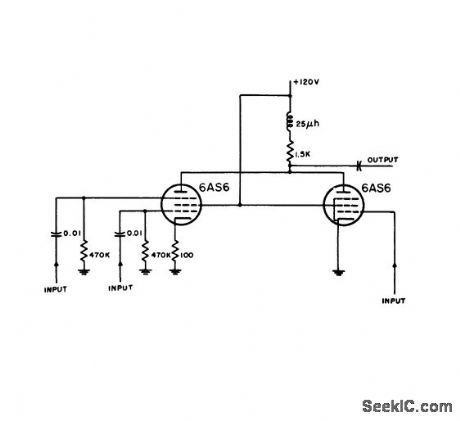
DUAL_GRID_PENTODE_MIXER
Published:2009/7/23 23:42:00 Author:Jessie
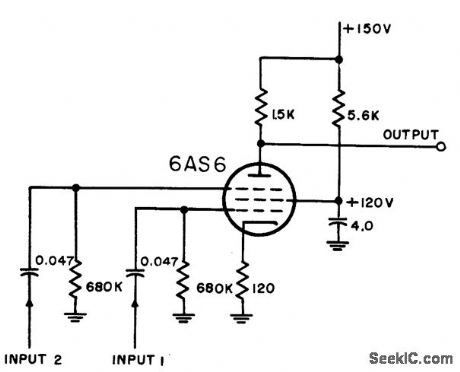
Uses 6AS6, in which suppressor grid has cutoff characteristic similar to control grid. Pulses of higher amplitude, such as markers, should be impressed on suppressor grid, since its transconductance is about one-fourth that of control grid. Chief drawback is need for large screen bypass capacitor.-NBS, Handbook Preferred Circuits Navy Aeronautical Electronic Equipment, Vol. 1, Electron Tube Circuits, 1963, p N4-9. (View)
View full Circuit Diagram | Comments | Reading(2586)
MIXER_LIMITER
Published:2009/7/23 23:42:00 Author:Jessie

Common-plate mixer uses diode-limiting coupling circuit to nullify adding feature. Bias voltage on diode sets limiting level-NBS, Handbook Preferred Circuits Navy Aeronautical Electronic Equipment, Vol. 1, Electron Tube Circuits, 1963, p N4-8. (View)
View full Circuit Diagram | Comments | Reading(970)
Basic_dc_stabilized_composite_amplifier
Published:2009/7/23 23:41:00 Author:Jessie
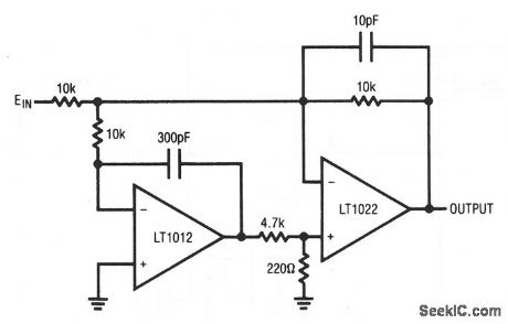
This composite amplifier combines the LT1012's 35-μV offset and 1.5 V/℃ drift, with the LT1022's 24 V/μs slew rate and 300-kHz full power bandwidth, to provide both high speed and low drift/offset. Input bias is about 100 pA. (View)
View full Circuit Diagram | Comments | Reading(801)
MICROPROCESSOR_POWER_SUPPLY_WATCHDOG
Published:2009/7/3 2:59:00 Author:May
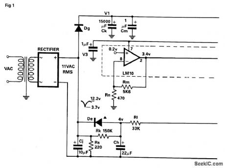
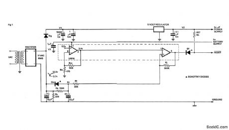
Circuit Notes
The circuit monitors the input to the microprocessor 5 V regulated supply for voltage drops and initiates a reset sequence before supply regulation is lost. In operation, the resistor capacitor combination Rs and Cj form a short time constant smoothing network for the output of the fullwave bridge rectifier. An approximately triangular, voltage waveform appears across C and Rs and it is the minimum excursion of this that initiatesthe reset. Diode Dg prevents charge sharing between capacitors Cj and Ck. Resistors Rn and Rm form a feedback network around the voltage reference section of the LM10C, setting a threshold voltage of 3.4 volts. The threshold voltage is set at 90% of the minimum voltage of the triangular waveform. When the triangular wave trough, at the comparator's non-inverting input, dips below the threshold, the comparator output is driven low. This presents a reset to the microprocessor. Capacitor Ch is charged slowly through resistor Rk and discharged rapidly through diode De. (View)
View full Circuit Diagram | Comments | Reading(740)
700_2000_Hz_TUNABLE_BANDPASS
Published:2009/7/3 2:58:00 Author:May
Uses RC notch circuit as feedback element for active-filter opamp. With tuning pot set for center frequency of 1000 Hz, 3-dB bandwidth is 23 Hz and 10-dB bandwidth is 68 Hz. At 1000 Hz, voltage gain is 36 dB. High-frequency rolloff is good, being 43 dB down at 2000 Hz, so circuh converts 1000-Hz square wave into sine wave. Artide gives design equations.-C. Hall, Tunable RC Notch Filter, Ham Radio, Sept. 1975, p 16-20. (View)
View full Circuit Diagram | Comments | Reading(1289)
BURGLAR_ALARM
Published:2009/7/3 2:58:00 Author:May
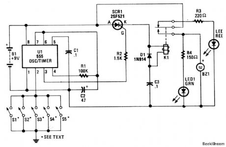
The heart of the circuit is a 555 oscillator/timer, U1, configured for monostable operation. The output of U1 at pin 3 is tied to the gate of SCR1. As long as S1-S5, which are connected to the trigger input of U1, are open, the circuit remains in the ready state, and does not trigger SCR1 into conduction. Because the relay is not energized, battery current is routed through the relay's normally-closed terminal and through current-limiting resistor R3 to LED2, causing it to light.However, when one of the switches (S1-S5) is closed, grounding U1 pin2, the output of U1 at pin 3 increases, activating SCR1. That energizes the relay, pulling the wiper of K1 to the normally-open termi-nal, causing LED1 to light and BZ1 to sound.The duration of the output is determined by the RC time-constant circuit, formed by R1 and C1.Resistor R2 regulates the output of U1 to a safe value for the gate of SCR1. Switches S1-S5 are to doors, windows, etc. A switch can be connected in series with B1 to activate and deactivate the alarm circuit when it's not needed. (View)
View full Circuit Diagram | Comments | Reading(0)
10_MHz_TRACKING
Published:2009/7/3 2:58:00 Author:May
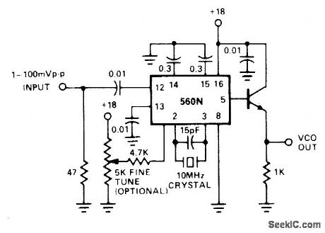
Connection shown for 560N PLL tracking filter uses crystal to keep free-runnlng frequency at desired value for Signals near 10 MHz Lock range varies with inputamplitude,from about 0.3 kHz for 1 mV P-P input to about 3 kHz for 100 mV P-P.- Signetics Analog Data Manual, signetics,Sunnyvale,CA,1977,p 850-851. (View)
View full Circuit Diagram | Comments | Reading(860)
BANDPASS_FOR_CW
Published:2009/7/3 2:57:00 Author:May
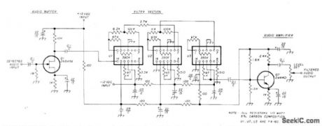
Sophisticated audio processing system for CW bandpass, using communication receiver, has actual bandpass center frequency between 900 and 950 Hz.Bandwidth is about 150 Hz Minimum relative attenuation is above 20 dB,Uses three KineticTechnology FX-60 ICs(cuned from FS-60,FS-65,and FS-61 production by manufacturer).-M. A.Chapman, Audio Filters for Improving SSB and CW Reception, Ham Radio, Nov.1976, p 18-23. (View)
View full Circuit Diagram | Comments | Reading(1444)
AUDIBLE_METER_READER
Published:2009/7/3 2:56:00 Author:May
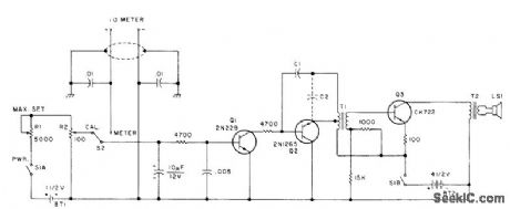
Analog meter terminals are connected to input of DC amplifier Q1 for feeding audio oscillator Q2 and output amplifier Q3. Frequency of oscillator is directly proportional to reading of meter. At calibrate position of S2, DC amplifier is fed by voltage divider R1-R2 and R2 is adjusted until tones heard are identical for both positions of S2. Developed for use by blind person. Knob of R2 sweeps over large scale having markings in Braille for reading of setting at which tones match. Alternatively, R2 can be preset to desired reading and equipment under test adjusted to give tone match. Article covers construction and calibration. C1 is chosen in range of 0.002 to 0.1 μF to give desired minimum fre quency. C2, if required, is in same range. T1 is transistor driver transformer (10,000 to 2000 ohms), and T2 is transistor output transformer (500 to 3.2 ohms).-N .Rosenberg, Tune-UpAids forthe Blind.73Magazine, Feb,1978,p64-67. (View)
View full Circuit Diagram | Comments | Reading(648)
LOW_VOLTS_ALARM
Published:2009/7/3 2:55:00 Author:May
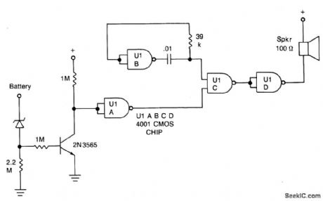
Circuit Notes
This inexpensive dc supply-voltage monitor sounds a warning when the voltage falls below a preset value. It is ideal for monitoring rechargeable batteries since it draws only a few microamperes when not sounding. The voltage at which the alarm sounds is determined by the zener diode. When the voltage falls below the zener voltage, the alarm sounds. The alarm tone is determined by the RC time constant of the 39 k resistor and 0.01 mf capacitor. (View)
View full Circuit Diagram | Comments | Reading(1023)
05MHz_WITH_100_DEVIATION_
Published:2009/7/3 2:55:00 Author:May
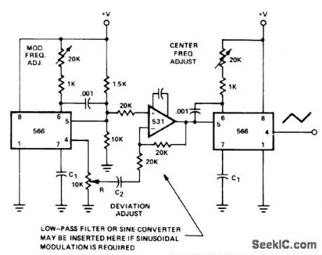
Carrier frequency under 0.5 MHz is generated by 566 function generator at right, for modulation by other 566 connected as triangle generator whose output is boosted by 531 opamp to give deviations up to ±100% of carrier frequency. Capacitors C1 control frequency range of each function generator.- Signetics Analog Data Manual, Signetics, Sunnyvale, CA, 1977, p 852-854. (View)
View full Circuit Diagram | Comments | Reading(1328)
1_kHz_BANDPASS_NOTCH
Published:2009/7/3 2:54:00 Author:May
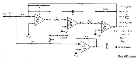


Biquad filter uses all four sections of LM324 quad differential-input opamp to provide choice of bandpass and notch outputs. Supply voltage range can be 3-32 v, with reference voltage equal to half of supply value used. For center frequency of 1 kHz,R is 160K, C is 0.001 μF, and R1-R3 are 1.6 megohms,Coupling capactions C1 can be 10 times value used for C.- Low Power Operational mplifiers, Motorola,Phoenix,AZ,1978,DS9339 R1. (View)
View full Circuit Diagram | Comments | Reading(1689)
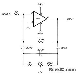
SECOND_ORDER_1_kHz_LOW_PASS
Published:2009/7/3 2:52:00 Author:May
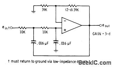
Circuit using 741 opamp has equalvalue series input resistors and high-pass capacitors. Cutoff frequency can be increased by changing 10K resistors to higher values while keeping their values identical. 10:1 resistance change provides 10:1 frequency change. Damping d is adjustable; critical value of 1.414 gives maximum flatness of response without overshoot. Interchange 10K resistors and 0.016-μF capacitors to convert circuit to 1-kHz high-pass filter.-D. Lancaster, Active-Filter Cookbook, Howard W. Sams, indianapolis, IN, 1975, p 127-129. (View)
View full Circuit Diagram | Comments | Reading(997)
15_A_negative_fixed_current_regulator
Published:2009/7/23 23:44:00 Author:Jessie
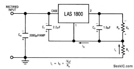
This circuit uses the LAS1800 series voltage regulator (Fig. 7-42A) as a fixed-current regulator. Characteristics are shown in Fig. 7-42B, 7-42C, and 7-42D. (View)
View full Circuit Diagram | Comments | Reading(615)
FONT_face=VerdanaRSUB1_SUB_RSUB2_SUB_–_VSUB1_SUB_VSUB2_SUB_FONT_frequency_converter
Published:2009/7/23 23:44:00 Author:Jessie
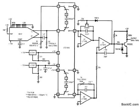
Fig, 12-16 This circuit produces an output frequency that is proportional to the ratio of voltages across two external resistors. The circuit has wide application in transducer signal-conditioning (chapter 14). Both R1 and R2 are ground-referred for noise considerations. In this particular circuit, R1 is a platinum resistance sensor and R2 is set at the R1 0℃ value. The circuit may be used with any resistive-based transducer. For negative TC devices, reverse the positions of R1 and R2. The grounded end of R2 allows fine trimming with decade boxes (if necessary to compensate for R1 tolerances at 0°) without excessive noise problems. The grounded side of R1 permits RI to be located at the end of a cable run (again without noise problems). The DAC serves as a simple source of two identical currents (The DAC MSB is set high, with all other bits low). With constant and equal currents, R1 and R2 produce a differential voltage, which is sampled by the LTC1043 switched-capacitor in the normal manner. To trim, place R1 in a 100℃ environment and adjust the full-scale trim for a 1-kHz output. Linear Technology. Linear Applications Handbook, 1990 p. AN14-17. (View)
View full Circuit Diagram | Comments | Reading(833)
15_A_negative_adjustable_voltage_regulator
Published:2009/7/23 23:44:00 Author:Jessie
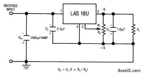
The LAS18U is a four-terminal adjustable regulator IC with an output range from -2.6 to -30 V, adjustable from a single pot. Characteristics are shown in Fig. 7-42B, 7-42C, and 7-42D. (View)
View full Circuit Diagram | Comments | Reading(791)
THREE_INPUT_TWO_PENTODE_MIXER
Published:2009/7/23 23:44:00 Author:Jessie
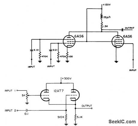
Distance markers and iff signals are inserted at separate grids on one tube, while radar video from input 3 is impressed on control grid of other pentode.-NBS, Handbook Preferred Circuits Navy Aeronautical Electronic Equipment, Vol. l, Electron Tube Circuits, 1963, p N4-4. (View)
View full Circuit Diagram | Comments | Reading(1158)
PREFERRED_AMPLIFICATION_15_PREAMPLIFIER
Published:2009/7/23 23:44:00 Author:Jessie
Used with instrument servo motor controller to increase available gain. Choice of pre-amplifier depends on error voltage per degree error available. Chopper is used with d-c inputs only.-NBS, Handbook Preferred Circuits Navy Aeronautical Electronic Equipment, Vol. I, Electron Tube Circuits, 1963, PC71,p 71-2. (View)
View full Circuit Diagram | Comments | Reading(659)
Wideband_FET_input_composite_buffer_
Published:2009/7/23 23:44:00 Author:Jessie
This composite circuit provides a gain of 0.95 with a full power bandwidth near 50 MHz and a slew rate of 2000 V/μs. Offset is about 5μV. Figure 1-19B shows a delay between input and output of about 4 ns. (View)
View full Circuit Diagram | Comments | Reading(758)
PREFERRED_COMMON_CATHODE_MIXER
Published:2009/7/23 23:43:00 Author:Jessie
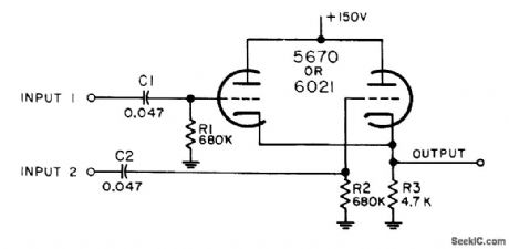
Combines video signals and pulses from two inputs, as for radar video, beacon signals, range markers, range strobes, and azimuth markers. Mixer is nonadditive and noninverting, can handle fast rise times, but amplification is less then unity and it cannot handle negative inputs.-NBS, Handbook Preferred Circuits Navy Aeronautical Electronic Equipment, Vol. I, Electron Tube Circuits, 1963, PC 23, p 23-2. (View)
View full Circuit Diagram | Comments | Reading(825)
| Pages:1121/2234 At 2011211122112311241125112611271128112911301131113211331134113511361137113811391140Under 20 |
Circuit Categories
power supply circuit
Amplifier Circuit
Basic Circuit
LED and Light Circuit
Sensor Circuit
Signal Processing
Electrical Equipment Circuit
Control Circuit
Remote Control Circuit
A/D-D/A Converter Circuit
Audio Circuit
Measuring and Test Circuit
Communication Circuit
Computer-Related Circuit
555 Circuit
Automotive Circuit
Repairing Circuit