
Circuit Diagram
Index 1120
LOW_COST_SPEED_REGULATOR_FOR_DC_MOTORS
Published:2009/7/3 3:05:00 Author:May
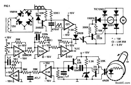
A four thyristor controlled bridge is used for operation in two quadrants of the torquespeed characteristics. In the trigger circuits the usual pulse transformers were replaced by self biased circuits which minimize gate power consumption and increase noise immunity. Electrical isolation is guaranteed by the use of optocouplers. The trigger pulses are generated by the comparison between an error signal, previously processed and amplified, and a line synchronism signal. The converter's output is a dc voltage proportional to the speed, which after being compared with a reference signal, becomes the error signal. (View)
View full Circuit Diagram | Comments | Reading(1474)
ABSOLUTE_VALUE_NORTON_AMPLIFIER
Published:2009/7/3 3:04:00 Author:May
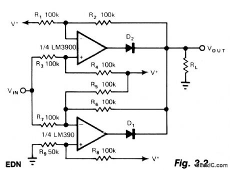
The noninverting amplifter has a gain of R2/R3 (1 in this case) and produces a voltage of Vout during a positive excursion of Vin with respect to ground.The inverting amplifter accommodates the negative excursions of Vin; its gain is given by -R6/R7, which equals -1 to maintain symmetry with the noninverting amplifter. R9 provides adjustment for the symmetry, supply variations, and offsets. Even though the circuit operates on a single supply, Vin can go negative to the same extent that it goes positive. (View)
View full Circuit Diagram | Comments | Reading(969)
COMPLEME_NTARY_TRANSISTOR_SERVO_AMPLIFIER
Published:2009/7/23 23:47:00 Author:Jessie

Use of direct coupling eliminates transformers. For d-c loads, C1 and C3 must be shorted. Will drive 20 V rms into 40-ohm load, giving 10 W. Voltage gain is 37 db and power gain is 60 db.-N. Freyling, High Performance All Solid-State Servo Amplifiers, Motorola Application Note AN-225, Jan. 1966 (View)
View full Circuit Diagram | Comments | Reading(930)
STEPPING_MOTOR_DRIVER
Published:2009/7/3 3:03:00 Author:May

Stepping motors find wide use in disk drives and machine control. MOSPOWER transistors are ideal motor drivers because of their freedom from second breakdown. Note that snubbing networks are not used because load line shaping is not necessary with MOSPOWER and the inductance of the motor is fairly low so that the inductive spike is small. The MOSFET gates are tied directly to the outputs of the CMOS control circuitry. The logic is arranged to sequence the motor in accordance with the needs of the application. (View)
View full Circuit Diagram | Comments | Reading(946)
INPUT_OUTPUT_BUFFER_AMPLIFIER_FOR_ANALOG_MULTIPLEXERS
Published:2009/7/3 3:03:00 Author:May
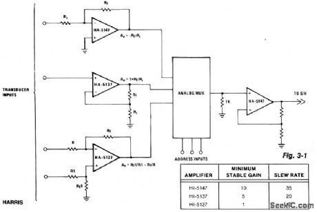

The precision input characteristics of the HA-5147 help simplify system error budgets, while its speed and drive capabilities provide fast charging of the multiplexer's output capacitance. This speed eliminates an increased multiplexer acquisition time, which can be induced by more limited amplifiers. The HA-5147 accurately transfers information to the next stage while effectively reducing any loading effects on the mul-tiplexer's output. (View)
View full Circuit Diagram | Comments | Reading(713)
Positi_to_negative_dc_dc_inverter
Published:2009/7/23 23:47:00 Author:Jessie
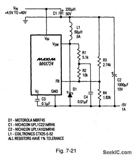
Figure 7-21 shows the MAX724 connected to provide -5 V at a 1-A output with a+4.5-V to+40-V input.See Figs.7-18 and 7-19 for pln configurations and Fig.7-20 for component suppliers,MAXIM EVALUATION KIT DATA Book,1994 P.3-138. (View)
View full Circuit Diagram | Comments | Reading(740)
PWM_MOTOR_SPEED_CONTROL
Published:2009/7/3 3:03:00 Author:May
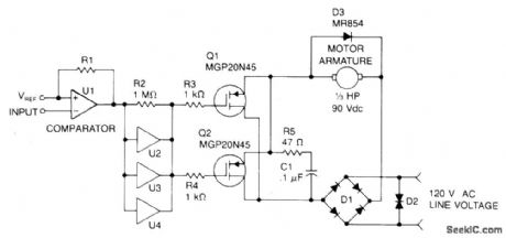
Speed control is accomplished by pulse width modulating the gates of two MGP20N45 TMOS devices. Therefore, motor speed is proportional to the pulse width of the incoming digital signal, which can be generated by a microprocessor or digital logic.The incoming signal is applied to comparator U1, then to paralleled inverters U2, U3, and U4 that drive the two TMOS devices, which, in turn, control power applied to the motor armature. Bridge rectifier Dl supplies fullwave power that is filtered by R5 and C1. Free-wheeling diode D3 (MR854) prevents high voltage across Q1 and Q2.A back-to-back zener diode, D2, protects against transients and high voltage surges. (View)
View full Circuit Diagram | Comments | Reading(1241)
Fast_dc_stabilized_noninverting_amplifier
Published:2009/7/23 23:46:00 Author:Jessie
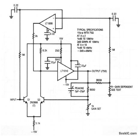
This circuit combines an LT1010 (and a fast discrete stage) with an LT1008-based dc-stabilizing loop. The output depends on the setting of the gain pot. Typical specifications are shown for voltage gains of 2 and 10. The normal tendency of the Q1/Q2 stage to drift is corrected by the LT1008. This correction stage is similar to those of Figs. 1-19 and 1-20, except that the feedback is taken from a divided-down sample of the fast amplifier. The ratio of this divider should be set (by the selection of the gain-dependent resistor) to the same value as the circuit closed-loop gain (typically 2 or 10). The output is typically 1 VPP (suitable for video), and should be adjusted for optimum (with a load applied) using the peaking capacitor.
(View)
View full Circuit Diagram | Comments | Reading(763)
1_kHz_BANDPASS_HIGH_Q
Published:2009/7/3 3:02:00 Author:May

Shunt-switched bandpass filter with o of 1000 and voltage gain of about 7 uses DG508 CMOS multiplexer containing required analog switches,interface cicuhs, and deoode logic for 8-path filter. Bandwidth for 3 dB down is 1 Hz centered on 1 kHz, with asymptotic slope of 6 dB per octave. Clock controls shunt-switched filter action.- Analog switches and Their Applications, Siliconix,Santa Clara,CA,1976,p 5-12-5-14. (View)
View full Circuit Diagram | Comments | Reading(1084)
BI_DIRECTIONAL_PROPORTIONAL_MOTOR_CONTROL
Published:2009/7/3 3:01:00 Author:May
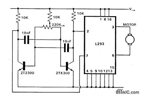
The control of both direction and of proportional motor speed is achieved by rotation of a single potentiometer. The motor driver is an SGS integrated circuit L293 which will drive up to 1 amp in either direction, depending on the logic state of input 1 and input 2 as per table.
I/P1 I/P2 FunctionHigh Low Motor turns one way Low High Motor reverses
By applying a variable M/S ratio flip-flop to these inputs, both speed and direction will be controlled. With RV1 in its center position the M/S will be 1:1 whereby the motor will remain stationary due to its inability to track at the flip-flop frequency. Movement of RV1 in either direction will gradually alter the M/S ratio and provide an average volt-age bias in one direction proportional to the M/S ratio. (View)
View full Circuit Diagram | Comments | Reading(2287)
15_A_negative_adjustable_current_regulator
Published:2009/7/23 23:45:00 Author:Jessie
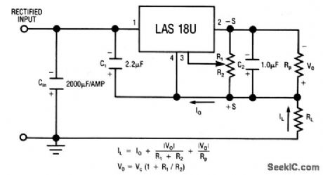
This circuit uses the LAS18U voltage-regulator IC (Fig.7-43) as an adjustable-current regulator. Characteristics are shown in Fig. 7-42B, 7-42C, and 7-42D. (View)
View full Circuit Diagram | Comments | Reading(750)
OPERATIONAL_PREAMPLIFIER
Published:2009/7/23 23:45:00 Author:Jessie
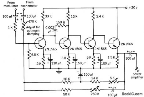
Used to sum modulator and tachometer outputs and provide signal for power amplifier that drives split-phase motor. Adjustable overall d-c feedback insures equal clipping when amplifier is overloaded, so squared output will have equal mark-space ratio.-Texas Instruments Inc., Transistor Circuit Design, McGraw-Hill, N.Y., 1963, p 493, (View)
View full Circuit Diagram | Comments | Reading(780)
Gain_trimmable_wideband_FET_amplifier
Published:2009/7/23 23:45:00 Author:Jessie
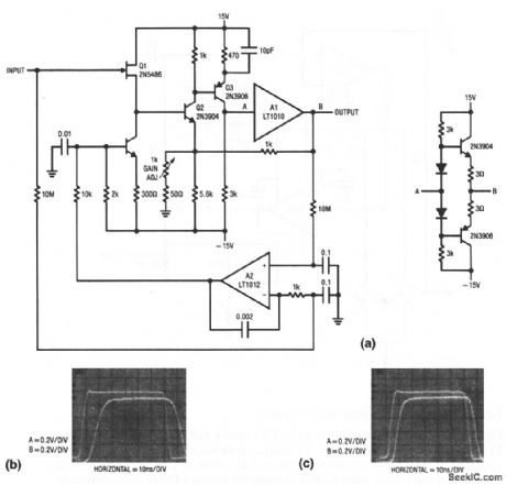
This circuit is similar to that of Fig. 1-19, except that voltage gain can be trimmed (to full unity gain, or to a gain of 10, etc.). With a 1-kΩ gain adjust set to unity, power bandwidth (1 Vpp) is 10 MHz, and slew rate is 100 V/μs. With the voltage gain set at 10, power bandwidth stays at 10 MHz, while the -3-dB point drops to about 22 MHz (from about 35 MHz at unity gain). With the optional discrete stage, slew rate exceeds 1000 V/μs, full power bandwidth is 18 MHz, and the -3-dB point is 58 MHz. With a voltage gain of 10, full power is available to 10 MHz, with the -3-dB point at 36 MHz. Figures 1-20B and 1-20C show the response with the LT1010 output, and the discrete output, respectively. As shown, the discrete stage is slightly faster (less delay between input and output). (View)
View full Circuit Diagram | Comments | Reading(956)
60_CPS_SERVO_AMPLIFIER
Published:2009/7/23 23:45:00 Author:Jessie
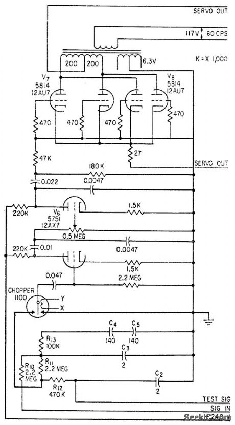
Consists of 60-cps d-c chopper, two stages of 60-cps voltage amplification V6, and 4-W power output stage V7-V8 that drives control winding of two-phase servo motor. Over-all power gain is 80 db.-P. G. Balko, Infrared Finds Audio Suspension Leaks, Electronics, 31:49, p 82-85. (View)
View full Circuit Diagram | Comments | Reading(720)
JOGGER_DATA_COLLECTlON
Published:2009/7/3 3:01:00 Author:May
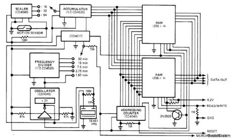
Portable data acquisition system using microcomputer to drive digital cassette tape transport operates from 12-V rechargeable battery and fits in backpack having total weight of only 8 Ib. Sample rate can be set between 20 and 100 Hz, with 2 min of continuous data being stored at fast rate. Recorded data is played into PDP-11 minicomputer later for analysis. Motion sensor shown can be replaced by other types of transducers for mea uring desired physiological phenomena during jogging, walking, or running.-P. G. Schreier, Physiological Data Acquisition Presents Unusual Problems, Solutions, EDN Magazine, June 20, 1978, p 25-26, 28, and 30. (View)
View full Circuit Diagram | Comments | Reading(755)
Cable_length
Published:2009/7/23 23:42:00 Author:Jessie
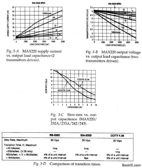
The old RS-232C interface specification calls for a maximum cable length of 50 feet.The newer EIA-232D specification calls for a length of cable that produces a capacitance of 2500 pF. This change from feet of cable to pF of load capacitance recognizes one of the problems in RS-232C. Not only does RS-232C ignore the effects of cable capacitance, but it contains a 50-ft distance limit that is often ignored by designers.
The EIA-232D specification considers cable length indirectly, through the effect of load capacitance, but does not specify a maximum length. Because the capacitance of inexpensive cable can range from 12 pF/ft for a single twisted pair to 30 pF/ft for low-noise shielded, multiple-twisted-pair cable, there is some confusion.
Cable capacitance is important because EIA-232D transmission are ac signals. Higher capacitance demands higher peak currents from the transmitter, resulting in higher average supply current for a given data rate, as shown in Fig. 3-A. Also, the cable impedance forms an ac divider with the transmitter output impedance. Higher cable capacitance lowers the divider shunt component. In turn, this reduces signal amplitude at the receiver end of the cable, as shown in Fig. 3-B. This signal loss becomes a problem when the receiver-end voltage falls below the specified 5-V minimum input level (required by most digital equipment).
Finally, cable capacitance limits the slew rate available from a given transmitter, as shown in Fig. 3-C. The slew rate determines the transition time between the +3-V and -3-V signal levels. (Slew rate is discussed further in Chapter 6.) Transition time limits the maximum data rate according to the specifications in RS-232C, EIA-232D, and CCITT V28, as shown in Fig. 3-D.
The simplest way to calculate the maximum allowable cable length for an EIA-232D interface IC (transceiver) is to divide the 2500-pF load specification by the capacitance per foot specified for the cable. Then, for cable lengths up to that limit, you can rest assured that the transceiver will operate properly and provide the maximum specified data rate.
Figure 3-E shows how the data rate can be extended past the specification limits. Longer cable adds to the line capacitance, lengthening the signal transition time, thus limiting the data rate. However, you can implement cable lengths and data rates well beyond the limits implied by the EIA-232D specification. (View)
View full Circuit Diagram | Comments | Reading(813)
CARRIER_OPERATED_RELAY_
Published:2009/7/3 3:00:00 Author:May
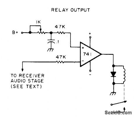
Relay is energized when carrier is present in FM receiver, to activate transmitter for repeater applications or turn on tape recorders, alarms, or other devices.Will work with either solid-state or tube-type receivers. Inverting (minus) input of opamp is connected directly to collector of audio preamp transistor or any other point having voltage change between signal and nosignal. If voltage change is in wrong direction, reverse leads to opamp input. Use 1K pot to set reference voltage so relay trips reliably on incoming signal.Relay can be reed-type drawing less than 75 mA.-S. Uhrig, The 5 Minute C0R, 73 Magazine, Dec. 1976, p 152-153. (View)
View full Circuit Diagram | Comments | Reading(3413)
BURGLAR_ALARM_2
Published:2009/7/3 3:00:00 Author:May
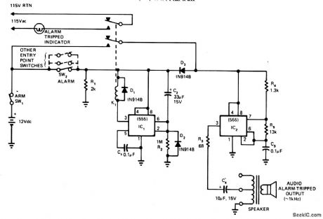
This circuit cannot be shut off for 10 to 60 seconds-even if the trip condition is immediately removed.It draws no standby power from the battery and is self-resetting.
(View)
View full Circuit Diagram | Comments | Reading(676)
300_3000_Hz_TUNABLE_FOUR_FUNCTION
Published:2009/7/3 3:00:00 Author:May
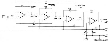
Provides choice of high-pass, bandpass, low-pass, and tunable notch outputs. Uses National LM324 quad opamp. Tuning pots are ganged 500K 2-W carbon with reverse log taper. Notch of -35 dB is 200 Hz wide at -3 dB points. Notch output has unity gain with respect to input signal, but other three outputs provide gain.-P.A. Lovelock, Discrete Operational Amplifier Active Filters, Ham Radio, Feb.1978, p 70-73. (View)
View full Circuit Diagram | Comments | Reading(1715)
Fast_dc_stabilized_composite_amplifier
Published:2009/7/23 23:42:00 Author:Jessie
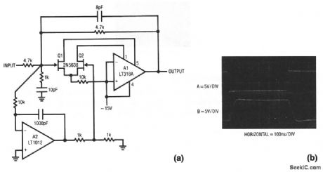
This composite amplifier is similar to that of Fig. 1-17, except that FETs are used to increase speed. Full power bandwidth is about 1 MHz, with a slew rate over 100 V/μs. Input bias is about 100 pA, offset and drift are about the same as Fig. 1-17. Figure 1-18B shows pulse response (trace A is input, trace B output).
(View)
View full Circuit Diagram | Comments | Reading(693)
| Pages:1120/2234 At 2011011102110311041105110611071108110911101111111211131114111511161117111811191120Under 20 |
Circuit Categories
power supply circuit
Amplifier Circuit
Basic Circuit
LED and Light Circuit
Sensor Circuit
Signal Processing
Electrical Equipment Circuit
Control Circuit
Remote Control Circuit
A/D-D/A Converter Circuit
Audio Circuit
Measuring and Test Circuit
Communication Circuit
Computer-Related Circuit
555 Circuit
Automotive Circuit
Repairing Circuit