
Circuit Diagram
Index 1107
SHUNT_PEAKED_INTERSTAGE
Published:2009/7/23 23:31:00 Author:Jessie
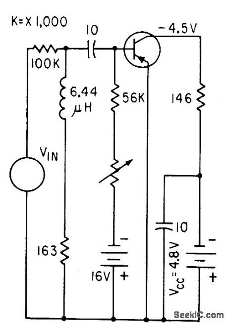
Pole-zero cancellation design procedure for using shunt peaking gives simple cascaded broadband video amplifier. Gain is 10.4 and bandwidth is 1.05 Mc.-R. 5. Pepper and D. O. Pederson, Designing Shunt-Peaked Transistor Amplifiers, Electronics, 33:49, p 68-70. (View)
View full Circuit Diagram | Comments | Reading(636)
TRANSFORMER_COUPLED_SERVO_AMPLIFIER
Published:2009/7/23 23:31:00 Author:Jessie
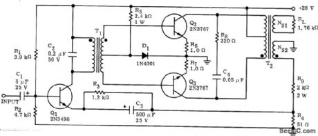
Three transistors provide stable voltage gain of 40 db and power gain of 37 db. Maximum output is 115 V rms into 1,760-ohm load, for 7.5 W.-N. Freyling, High Performance All Solid. State Servo Amplifiers, Motorola Application Note AN-225, Jan.1966. (View)
View full Circuit Diagram | Comments | Reading(877)
15_A_positive_adjustable_current_regulator
Published:2009/7/23 23:30:00 Author:Jessie
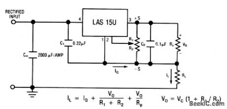
This circuit uses the LAS15AU voltage-regulator IC (Fig. 7-33) as an adjustable-current regulator. Characteristics are shown in Fig. 7-32B, 7-32C, and 7-32D. (View)
View full Circuit Diagram | Comments | Reading(602)
FOUR_INPUT_HIGH_LEVEL_PULSE_MIXER
Published:2009/7/23 23:30:00 Author:Jessie
Triode in series with plate load of mixer pro vides for additional blanking pulse.-NBS Handbook Preferred Circuits Navy Aeronoutical Electronic Equipment, Vol.1, Electron Tube Circuits, 1963, p N4-3. (View)
View full Circuit Diagram | Comments | Reading(709)
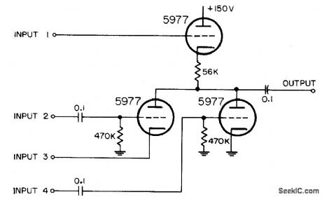
THREE_PENTODE_MIXER
Published:2009/7/23 23:30:00 Author:Jessie
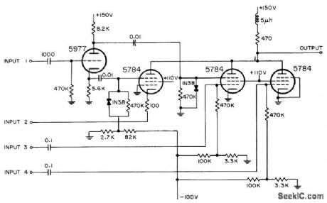
Triode is used as phase splitter. Both positive and negative signals are combined from four inputs. High-frequency compensation is used in common plate circuit of pentodes.-NBS, Handbook Preferred Circuits Navy Aeronautical Electronic Equipment, Vol. 1, Electron Tube Circuits, 1963, p N4-5. (View)
View full Circuit Diagram | Comments | Reading(699)
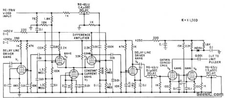
SERVO_AIMS_D_F_LOOP_AUTOMATICALLY
Published:2009/7/23 23:30:00 Author:Jessie
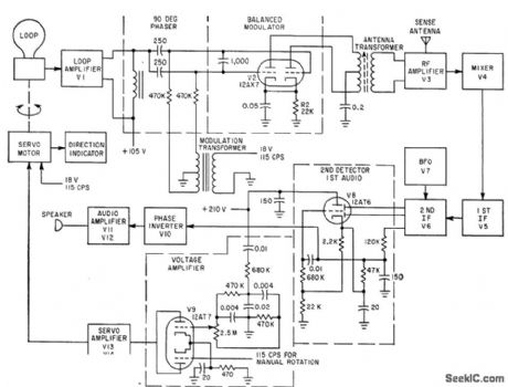
Bearing accuracy of 3 deg is obtained over frequency range of 190 kc to 2.8 Mc, Error-signals derived from balanced modulator and sense antenna are mixed, amplified, defected by V8, and amplified to drive two-phase antenna motor-L. D. Shergalis, Pleasure Boat Electronics Stresses Low Power Consumption, Operating Simplicity, Electronics, 35:4, p 20-21. (View)
View full Circuit Diagram | Comments | Reading(857)
15_A_positive_fixed_current_regulator
Published:2009/7/23 23:30:00 Author:Jessie
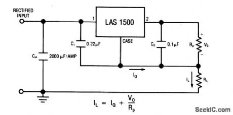
This circuit uses the LAS1500 series voltage regulator (Fig.7-32A) as a fixed-current regulator. Characteristics are shown in Fig. 7-32B, 7-32C, and 7-32D. (View)
View full Circuit Diagram | Comments | Reading(553)
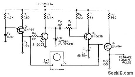
VERTICAL_LOCATOR_FOR_CHARACTER_READER
Published:2009/7/23 23:03:00 Author:Jessie
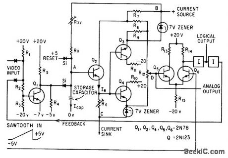
Sawtooth input is compared with earliest video of each vertical sweep of typed character being scanned, to charge capacitor and derive logical output related to bottom of typed line.-J. Bauldreay and E. Milbradt, Solving Registration Problems in Optical Character Recognition, Electronics, 35:1, p 77-81. (View)
View full Circuit Diagram | Comments | Reading(722)
Simple_adjustable_linear_regulator
Published:2009/7/23 23:03:00 Author:Jessie
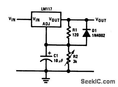
This circuit has a 1.2- to 25-V output range, set by R2. C1 improve ripple rejection. D1 prevents power surges (over 25-V output) from damaging capacitors. (View)
View full Circuit Diagram | Comments | Reading(649)
PULSED_30_W_TRANSMITTER
Published:2009/7/23 23:03:00 Author:Jessie
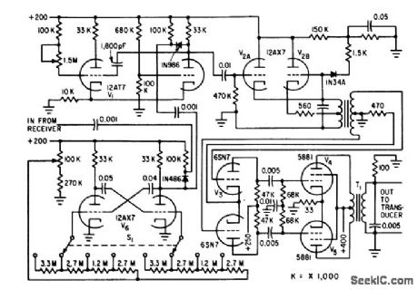
Uses pulsed Hartley oscillator operating at either 85 or 135 kc, followed by push-pull driver amplifier, push-pull power amplifier, and power amplifier that feeds 72-ohm transducer through step-down transformer Q1. Oscillator operates for 1-millisec period controlled by V1, which in turn is triggered by negative pulse coming from receiver through free-running mvbr V6.-H. F. Messias, UItrasonics Measures Flow Velocity of Rivers, Electronics, 34:41, p 56-59.
(View)
View full Circuit Diagram | Comments | Reading(631)
Worldwide_single_chip_supply_with_parallel_operation
Published:2009/7/23 23:03:00 Author:Jessie
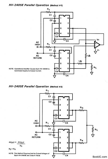
These two circuits show two HV-2405 single-chip supplies (Fig. 7-8) connected in parallel to increase current capability. (View)
View full Circuit Diagram | Comments | Reading(692)
Smgle_load_switch
Published:2009/7/23 23:03:00 Author:Jessie
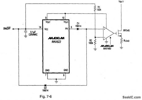
Figure 7-6 shows a MAX623 connected as a comparator-switch. The switch is turned on by applying VBATT to the ON/OFF input and turned off by pulling the input to ground. MAXIM NEW RELEASES DATA Book, 1992, P. 4-38.
(View)
View full Circuit Diagram | Comments | Reading(974)
UJT_RASTER_GENERATOR
Published:2009/7/23 23:02:00 Author:Jessie
Developed for use in low-cost transistorized flying-spot scanner. Can also be adapted for closed-circuit tv cam eras and monitors. Ujt Q1 is relaxation oscillator at desired horizontal sweep rate of 10 kc. Interlaced scanning is easily obtained.-F. Stevens, Low-Cost UJT Raster Generator, EEE, 13:12, p 65-66. (View)
View full Circuit Diagram | Comments | Reading(983)
Worldwide_single_chip_supply
Published:2009/7/23 23:02:00 Author:Jessie
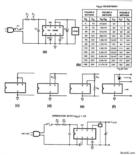
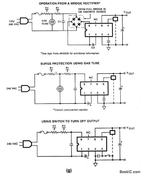
The HV-2405 converts ac into regulated dc, as described for the HV-1205 (Figs. 7-6 and 7-7), except that the HV-2405 operates from either 120 or 240 Vac (without special connections or a changeover switch). Recommended values for components shown in Figs. 7-8C through 7-8G are as follows: fuse F1=1/2 A, 2AG; R1=150 g; C1=0.05 μF, ac rated; MOV=V130LA20, or gas tube, which arcs at less than 500 V for 240 V use; C2, C3, C4, R2, RA, RB, and VZ are the same as for HV-1205. The HV-2405 does not provide isolation from the line (both ground and ac return are above ground). (View)
View full Circuit Diagram | Comments | Reading(897)
5_W_400_MHz_TM0S_FET_amplifier
Published:2009/7/23 23:01:00 Author:Jessie
This circuit uses an MRF134 and has a gain of 10.5 dB. (View)
View full Circuit Diagram | Comments | Reading(647)
NUCLEAR_TRACK_COUNTER
Published:2009/7/23 23:01:00 Author:Jessie
Recognition system scans nuclear emulsion strips coated on glass, using image orthicon with microscope. Straight or moderately curved tracks in emulsion, produced by nuclear particles, are recognized and counted by scanner that used video screening circuit shown. Opaque emulsion regions thee meet narrowness criteria produce output pulses.-P. V. C. Hough, J. A. Koenig, and W. Williams, Stunner Recognizes Atomic Particle Tracks, Electronics, 32:13, p 58-61. (View)
View full Circuit Diagram | Comments | Reading(971)
CB
Published:2009/7/23 23:01:00 Author:Jessie
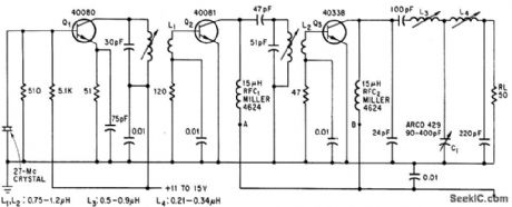
Three overlay transistors provide5 w for 27-Mc citizens-band a-m transmitter.-D. J. Donahue and B. A. Jacoby, Putting the Overlay to Work at High Frequencies, Electronics, 38:17, p 78-81.
(View)
View full Circuit Diagram | Comments | Reading(983)
TRF_RECEIVER
Published:2009/7/23 23:01:00 Author:Jessie
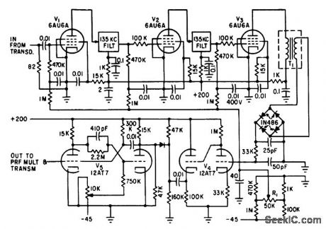
Operates at either 85 or 135 kc. Input impedance is 72 ohms to match transducer. Detected pulse of rectifier bridge is amplified in direct. coupled amplifier V4 and differentiated at its output, to trigger one-shot mvbr V5, which in turn triggers Transmitter and prf multiplier in computing circuitry.-H. F. Messias, Ultrasonics Meassures Flow Velocity of Rivers, Electronics, 34:41, p 56-59. (View)
View full Circuit Diagram | Comments | Reading(748)
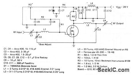
5_W_150_MHz_TMOS_FET_amplifier
Published:2009/7/23 23:00:00 Author:Jessie

This circuit uses an MRF134, has a gain of 14dB, and has a drain efficiency of 55%. The output amplitude can be adjusted by R3. (View)
View full Circuit Diagram | Comments | Reading(554)
Positive_and_negative_voltage_converter_1
Published:2009/7/23 23:07:00 Author:Jessie
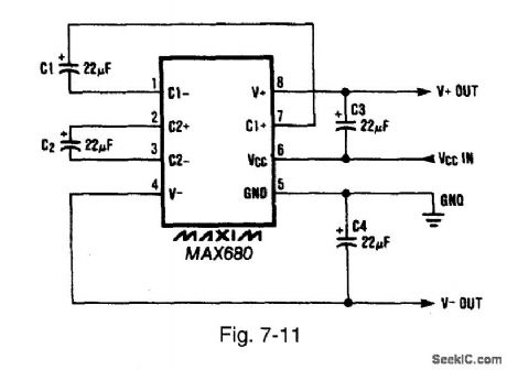
Figure 7-11 shows a MAX680 used as a positive and negative voltage converter. Capacitors C1 and C3 must be rated at 6 V or greater. Capacitors C2 and C4 must be rated at 12 V or greater. If the MAX680 is used for low-current applications, C1 and C2 can be reduced to 1 μF, and capacitors C3 and C4 can be reduced to 4.7μ F. MAXIM NEW RELEASES DATA Book, 1992, P. 4-144.
(View)
View full Circuit Diagram | Comments | Reading(2532)
| Pages:1107/2234 At 2011011102110311041105110611071108110911101111111211131114111511161117111811191120Under 20 |
Circuit Categories
power supply circuit
Amplifier Circuit
Basic Circuit
LED and Light Circuit
Sensor Circuit
Signal Processing
Electrical Equipment Circuit
Control Circuit
Remote Control Circuit
A/D-D/A Converter Circuit
Audio Circuit
Measuring and Test Circuit
Communication Circuit
Computer-Related Circuit
555 Circuit
Automotive Circuit
Repairing Circuit