
Circuit Diagram
Index 1105
25_W_UHF_amplifier_using_microstrip_techniques
Published:2009/7/23 22:52:00 Author:Jessie
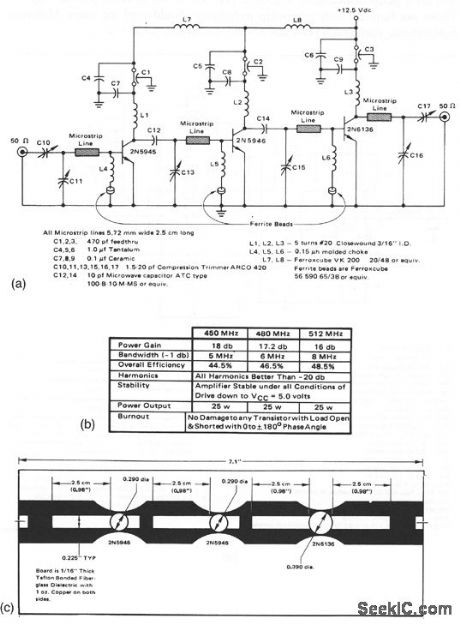
This circuit provides 25-W of output power in the 450- to 512-MHz UHF band, and is designed for 12.5-V operation. Figure 2-49B shows typical amplifier performance data. Figure 2-49C shows the microstrip board layout.Those not familiar with microstrip techniques should read the many Motorola publications, such as AN548A and AN555. (View)
View full Circuit Diagram | Comments | Reading(801)
CLASS_B_CB_TRANSCEIVER
Published:2009/7/23 22:52:00 Author:Jessie
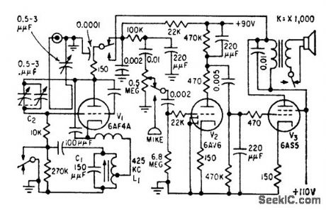
On transmit, V1 is self-excited power oscillator, V3 is am modulator, and V2 is speech amplifier. On receive, V1 is superregenerative r-f amplifier, V3 is audio power amplifier, and V2 is first audio stage.-L. G. Sands, Citizens Radio Re. vision Spurs Equipment Design, Electronics, 32:15, p 55-57. (View)
View full Circuit Diagram | Comments | Reading(1060)
UJT_TRIANGULAR_WAVE_GENERATOR
Published:2009/7/23 22:51:00 Author:Jessie
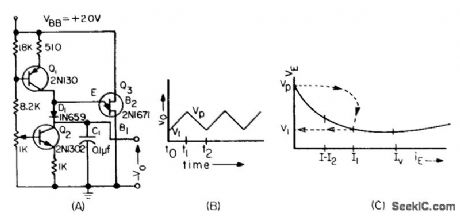
Two current generators produce triangular wave by alternately charging and discharging C1.Ujt and diode serve as switch to reverse slope of ramp.-R. Dean, Unijunction Triangular Wave Generator, EEE, 12:4, p 59. (View)
View full Circuit Diagram | Comments | Reading(2149)
Low_frequency_sine_wave_generator_with_quadrature_output
Published:2009/7/23 22:51:00 Author:Jessie
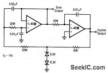
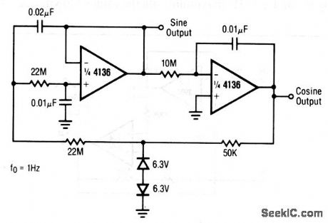
This circuit uses two sections of a 4136 op amp. The frequency of both the sine and cosine output is 1 Hz with the values shown. Raytheon Linear Integrated Circuits, 1989, p. 4-173. (View)
View full Circuit Diagram | Comments | Reading(1142)
NOISE_ACTUATED_AVC
Published:2009/7/23 22:50:00 Author:Jessie
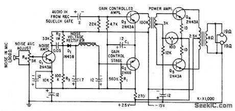
Emitter current of 2N43A controlled low-level audio amplifier stage Q3 is regulated indirectly by sound pressure level of ambient noise. With no noise, gain of controlled amplifier is prevented front going to zero by applying quiescent conduction bias through R1 to gain-control stage Q2.-D. C. Gibson, Helmet Transceiver for Flight Deck Communications, Electronics, 33:39, p 56-60. (View)
View full Circuit Diagram | Comments | Reading(635)
100_W_25_KC_ULTRASONIC_GENERATOR
Published:2009/7/23 22:50:00 Author:Jessie
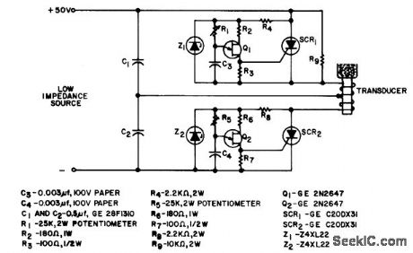
Frequency-doubling mode permits use of inexpensive scr's. Load resistance is in magnetostrictive transducer winding L. Circuit is actually 25-kc inverter triggered at 12.5-kc repetition rate.- Silicon Controlled Rectifier Manual, Third Edition, General Electric Co., 1964, p 16 (View)
View full Circuit Diagram | Comments | Reading(2701)
SIMPLE_UJT_SWEEP
Published:2009/7/23 22:50:00 Author:Jessie
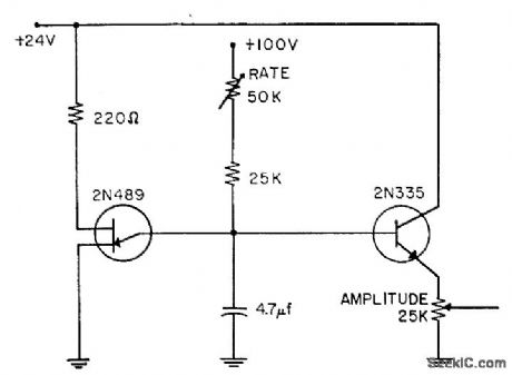
Generates variable-frequency sawtooth directly, with emitter-follower 2N335 serving only for isolation. Sawtooth frequency can be varied without affecting output amplitude.-Unijunction Sweep, EEE, 11:7, p 86. (View)
View full Circuit Diagram | Comments | Reading(820)
Wien_bridge_oscillator
Published:2009/7/23 22:50:00 Author:Jessie
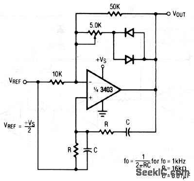
The frequency of VOUT is set by the values of R and C, as shown. Adjust the 5- kΩ potentiometer until the VREF point is one-half of the source voltage,VS. Raytheon Linear Integrated Circuts, 1989, p. 4-161. (View)
View full Circuit Diagram | Comments | Reading(2024)
THREE_TRANSISTOR_CB_TRANSCEIVER
Published:2009/7/23 22:50:00 Author:Jessie
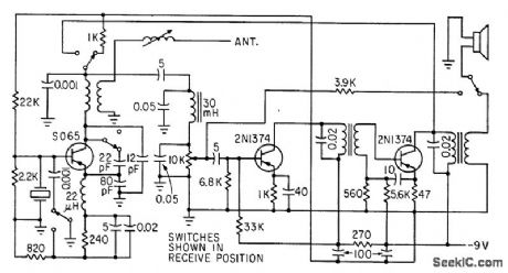
Has 30-mw r-f output and range of several thou. sand feet. Detector uses 40-kc quench. Draws 15 ma for receive and 30 ma for transmit. loudspeaker serves as microphone for transmitting.-L. Solomon, Gitizens Band Equipment Design, Electronics, 33:45, p 70-72. (View)
View full Circuit Diagram | Comments | Reading(719)
Adjustable_off_line_linear_supply
Published:2009/7/23 22:50:00 Author:Jessie
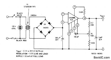
This circuit provides an output adjustable from 3.5 to 20 V, with a 90-mA load. Line and load regulation is 0.2%. Full-load ripple is 0.3 mV. (View)
View full Circuit Diagram | Comments | Reading(873)
Linear_amplifier_using_wideband_hybrids
Published:2009/7/23 22:50:00 Author:Jessie
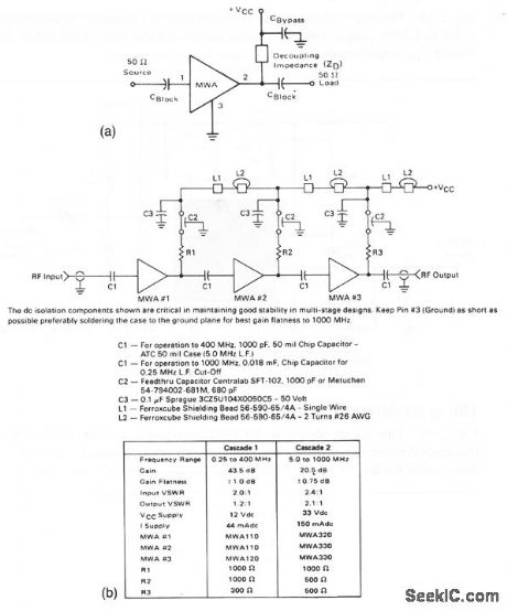
This circuit shows three wideband hybrid amplifiers cascaded to form a linear amplifier. Figure 2-48B shows the hybrid amplifier connections. As shown by the table, the circuit is capable of operation from 0.25 to 400 MHz (or 5 to 1000 MHz), depending on the selection of components and power sources. (View)
View full Circuit Diagram | Comments | Reading(718)
TRIANGULAR
Published:2009/7/23 22:49:00 Author:Jessie
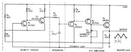
Deviation is less thon 1% from linearity at any frequency front 400 cps to 1 cycle per hour. Frequency is changed by varying R1, R2 or C; values shown give 20-second period. Used to sweep magnetic fold across air gap of electromagnet and for testing servos and vlf amplifiers.-J. r. Delpech, Triangular Waveforms Have 1 % linearity, Electronics, 38:7, p 86-87. (View)
View full Circuit Diagram | Comments | Reading(645)
Single_supply_RS_232_interface_for_bipolar_A_D_converters
Published:2009/7/23 22:46:00 Author:Jessie
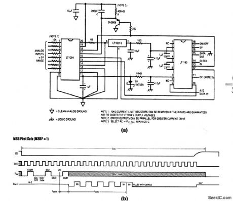
This circuit operates from a single 5-V supply, and draws a total quiescent current of about 37 mA. Figure 6-67B shows the operating sequence. The CS signal switches to a low state less than 1 μs after receiving the system clock, and the word can be transmitted after one cycle. After the 18 clock cycles required to complete conversion, the clock must shut off to allow CS to switch to a high state for at least 2 μs (minimum time between conversions). The operating sequence can then be repeated. (View)
View full Circuit Diagram | Comments | Reading(567)
Low_frequency_doubler
Published:2009/7/23 22:46:00 Author:Jessie
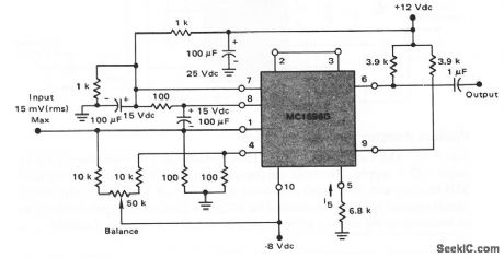
This circuit shows an MC1596 operating as a frequency doubler in the audio to 1-MHz range, with all spurious outputs greater than 30-dB below the desired 2fIN-output signals. (View)
View full Circuit Diagram | Comments | Reading(0)
CB_FILTER
Published:2009/7/23 22:46:00 Author:Jessie
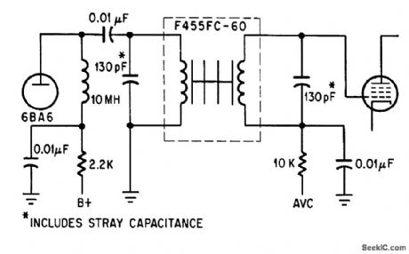
Electromechanical filler with 6-kc bandwidth at 455 kc gives 8 db signal-to-noise improvement.-Filtering the Chatter on Citizens' Band, Electronics, 38:5, p 81. (View)
View full Circuit Diagram | Comments | Reading(701)
Quadrature_oscillator
Published:2009/7/23 22:46:00 Author:Jessie
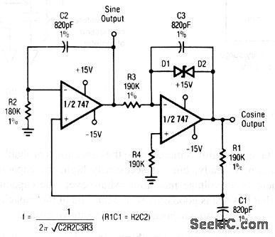
This circuit uses both sections of a 747 op amp. The frequency of the sine and cosine output is set by the values of R3, C3, R2, and C2, as shown. Raytheon Linear Integrated Circuits, 1989, p. 4-148. (View)
View full Circuit Diagram | Comments | Reading(962)
Double_balanced_mixer
Published:2009/7/23 22:45:00 Author:Jessie
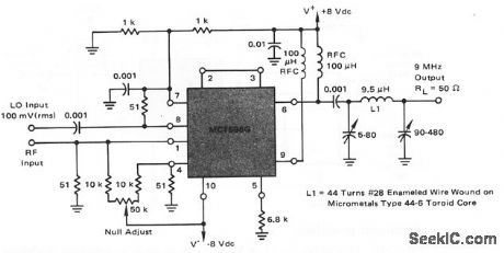
This circuit shows an MC1596 operating as a high-frequency mixer with a broadband input and a tuned output at 9 MHz. The 3-dB bandwidth of the 9-MHz output tank is 450 kHz. The local-oscillator (LO) signal of 100 mV is injected at pin 8, and the modulated-RF input of about 15 mV is injected at pin 1.For a 30-MHz input (pin 1) and a 39-MHz LO (pin 8), the mixer circuit has a conversion gain of 13 dB and an input sensitivity of 7.5μV for a 10 dB (S+N)/N ratio in the 9-MHz output signal. (View)
View full Circuit Diagram | Comments | Reading(0)
POSITIVE_OR_NEGATIVE_SLOPE
Published:2009/7/23 22:45:00 Author:Jessie

Generates linear ramps, either negative or positive, by switching two current sources on and off during charging of C3.-G. Marosi, Positive or Negative Slope Generator, EEE, 13:5, p 43. (View)
View full Circuit Diagram | Comments | Reading(776)
Unbalanced_dual_tracking_regulator
Published:2009/7/23 22:45:00 Author:Jessie
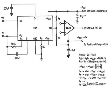
This circuit provides unbalanced output voltages that can be varied between ±50 mV and ±42 V by the selection of Ro, with load currents of ±200 mV This circuit is particularly useful for comparator applications. (View)
View full Circuit Diagram | Comments | Reading(770)
UNDERSEA_PROPAGATION_GATE_GENERATORS
Published:2009/7/23 22:44:00 Author:Jessie
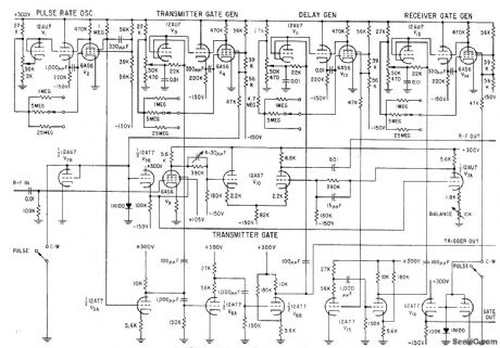
Pulse-rate oscillator V1 generates pulses with variable lime interval from 0.3 to 170 millisec for triggering rate. Normal operation is at 80 millisec, corresponding to 12.5 cps. Trigger pulses are amplified and delivered to circuits that trigger transmitter and delay generators for two receivers, and synchronize cm sweep. Used to measure changes in propagation time of less than 20 microsec over direct path of up to 300 feet in sea water.-W. C. Gore, Ultrasonics Tests Undersea Propagation, Electronics, 31:35, p 32-35. (View)
View full Circuit Diagram | Comments | Reading(711)
| Pages:1105/2234 At 2011011102110311041105110611071108110911101111111211131114111511161117111811191120Under 20 |
Circuit Categories
power supply circuit
Amplifier Circuit
Basic Circuit
LED and Light Circuit
Sensor Circuit
Signal Processing
Electrical Equipment Circuit
Control Circuit
Remote Control Circuit
A/D-D/A Converter Circuit
Audio Circuit
Measuring and Test Circuit
Communication Circuit
Computer-Related Circuit
555 Circuit
Automotive Circuit
Repairing Circuit