
Circuit Diagram
Index 1116
THERMISTOR_CONTROL
Published:2009/7/23 23:48:00 Author:Jessie

Thermistors RT1 and RT2 in series are heated equally under no signal. Applying ac signal increases resistance of one and lowers that of other, depending on phase. Q1 and Q2 form ac preamp. Q3 and Q4 operate in switched mode as demodulator. Circuit can be used in place of mechanical servo.-I. C. Hutcheon, Using Thermistors as Servo Elements, Electronics, 34:5, p 52-55. (View)
View full Circuit Diagram | Comments | Reading(749)
SCA_DEMODULATOR_
Published:2009/7/3 3:48:00 Author:May
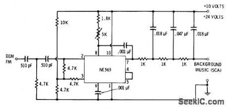
VCO of NE565 PLL is set at 67 kHz and is locked in by incoming 67-kHz subsidiary-carrier component used for transmitting unintewupted commercial background music by FM broadcast stations. Circuit demodulates FM sidebands and applies them to audio input of commercial sound system through suitable filter. 5K pot is used to lock VC0 exactly on frequency. Frequency response extends up to 7000 Hz.-E. M. Noll, Linear IC Principles, experiments, and Proiects, Howard VV. Sams, Indianapolis, IN, 1974, p 212-213. (View)
View full Circuit Diagram | Comments | Reading(1284)
PROGRAMMED_SERVO
Published:2009/7/23 23:38:00 Author:Jessie
Positions printed-circuit board in response to controller commands. Component selection and insertion are also directed by controller. Relays apply fine and coarse voltages to servo positioner as required.-S. B. Korin and F. B. Spencer, Programmed Servo Speeds Short-Run production, Electronics, 32:10, p 54-56. (View)
View full Circuit Diagram | Comments | Reading(758)
NONINVERTING_AMPLIFIER
Published:2009/7/3 3:48:00 Author:May

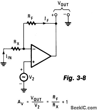
View full Circuit Diagram | Comments | Reading(0)
VOLTAGE_CONTROLLED_GAIN
Published:2009/7/23 23:38:00 Author:Jessie
Silicon diodes serve to vary gin of wideband video amplifier over range from 2 to 32 db, with bandwidth remaining almost constant at 12 Mc and input impedance constant at 10K.-R. S. Hughes, A Wideband Video Amplifier with Variable Gain, EEE, 12:8, p 54-55. (View)
View full Circuit Diagram | Comments | Reading(0)
AUTOMATIC_HEADLIGHT_DIMMER
Published:2009/7/3 3:47:00 Author:May

This circuit switches car headlights to the low beam state when it senses the lights of an on-coming car. The received light is very low level and highly directional, indicating the use of a lens with the detector. A relatively large amount of hysteresis is built into the circuit to prevent flashing lights. Sensitivity is set by the 22 megohm resistor to about 0.5 ft. candle at the transistor (0.01 at the lens), while hysteresis is determined by the R1, R2 resistor voltage divider, parallel to the D41K3 collector emitter, which drives the 22 megohm resistor; maximum switching rate is limited by the 0.t μF capaci-tor to 15/minute. (View)
View full Circuit Diagram | Comments | Reading(2976)
INVERTING_AMPLIFIER
Published:2009/7/3 3:47:00 Author:May
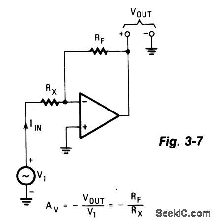
View full Circuit Diagram | Comments | Reading(0)
2_A_positive_adjustable_voltage_regulator
Published:2009/7/23 23:34:00 Author:Jessie
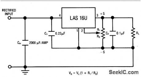
The LAS16U is a four-terminal adjustable regulator IC with an output range from +4 to+30 V, providing remote-sense capability with a single pot. Characteristics are shown in Fig.7-37B, 7-37C, and 7-37D. (View)
View full Circuit Diagram | Comments | Reading(808)
CASCADED_AMPLIFIER
Published:2009/7/3 3:46:00 Author:May
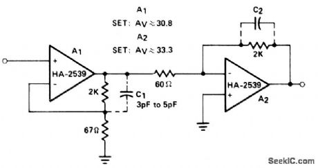
Cascaded amplifter sections are used to extend bandwidth and increase gain. Using two HA-2539 devices, this circuit is capable of 60-dB gain at 20 MHz. (View)
View full Circuit Diagram | Comments | Reading(1007)
Ultra_linear_V_F_converter
Published:2009/7/23 23:34:00 Author:Jessie
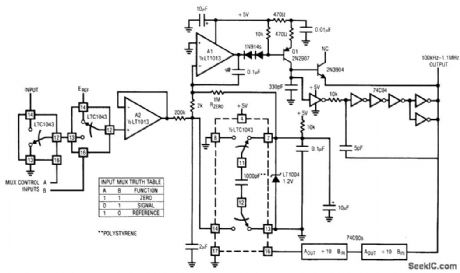
Fig. 12-10 Although this circuit can be used in a stand-alone mode, it is specifically intended for processor-driven applications, which require 17-bit accuracy, such as weighing scales. The circuit has a resolution of 1 ppm, with linearity inside 7 ppm (0.0007%). When combined with a processor-driven gain/zero calibration loop, the circuit has negligible zero and gain drift. A single 5-V supply is used to minimize interface problems. For processor operation, the input multiplexer (LTC1043) and RZERO (1 MΩ) must be added. With the multiplexer set to the ZERO function (see truth table) the A1 input is grounded, and the 200-kΩ.resistor receives no drive. However, At receives bias via RZERO and the circuit oscillates around 100 kHz. After reading this frequency, the processor shifts the multiplexer to the SIGNAL function, where the A2 output is a buffered version of the signal input. The circuit output frequency is now determined by this input, and the current through RZERO. Typical output range from 100 kHz to 1 MHz. Linear Technology. Linear Applications Handbook 1990 AN14-7. (View)
View full Circuit Diagram | Comments | Reading(799)
SERVO_MOTOR_DRIVE_AMPLIFIER
Published:2009/7/3 3:45:00 Author:May

Digital ICs and opto-isolators provide the drive for this TMOS servo amplifier, resulting in fewer analog circuits and less drift. Fast and consistent turn-on and turn-off characteristics also enable accurate analog output results directly from the digital signal without the need for analog feedback.An H bridge configuration is employed for the servo amplifier, which obtains complementary PWM inputs from digital control circuits. The PWM inputs are applied via opto-isolators, which keep the digital control logic isolated from the 75 V supply used for the amplifier. A short circuit indicator is provided by opto-isolator U3; if there is a short, the drop across R9 increases to a value sufficient to activate the isolator and send a short indication to the digital control logic. (View)
View full Circuit Diagram | Comments | Reading(3761)
TONE_OUTPUT_FOR_DIGITAL_DISPLAY
Published:2009/7/3 3:45:00 Author:May


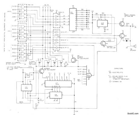
Converts BCD input from digital test gear to sequence of 10 different tones representing 0 to 9, for recognition of reading on digital display by blind radio operator or experimenter. Length of tone sequence equals number of digits displayed, plus sign indicator or half-digit if desired. Circuit shown is for 31/2 digits. Article describes operation of drcuit and gives construction details. Resistors R0-R9 (values inkilohms from 6.8K to 470K),determining frequencies of generated tones,are switched into VCO IC10 by IC9-D,R Pacholok,Digital to Audio Decoder,73 Magazine,Oct 1977,p 178-180. (View)
View full Circuit Diagram | Comments | Reading(838)
COMPOSITE_AMPLIFIER
Published:2009/7/3 3:45:00 Author:May


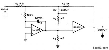

A composite configuration greatly reduces dc errors without compromising the high-speed, wideband characteristics of HA-2539. The HA-2540 could also be used, but with slightly lower speeds and band-width response.The HA-2539 amplifies signals above 40 kHz which are fed forward via C2; R2 and R5 set the voltage gain at -10. The slew rate of this circuit was measured at 350 V/μs. Settiing time to a 0.1% level for a 10-V output step is under 150 ns and the gain bandwidth product is 300 MHz.The HA-5170 ampliftes signals below 40 kHz, as set by C1 and R1, and controls the dc input charac-teristics such as offset voltage, drift, and bias currents of the composite amplifter. Therefore, it has an offset voltage of 100 μV, drift of 2 μV/'℃, and bias currents in the 20-pA range. The offset voltage can be externally nulled by connecting a 20-KΩ pot to pins 1 and 5, with the wiper tied to the negative supply.The dc gains of the HA-5170 and HA-2539 are cascaded; this means that the dc gain of the composite amplifier is well over 160 dB.The excellent ac and dc performance of this composite amplifter is complemented by its low noise performance, 0.5-μV rms from 0.1 Hz to 100 Hz. It is very useful in high-speed data acquisition systems. (View)
View full Circuit Diagram | Comments | Reading(0)
N_PHASE_MOTOR_DRIVERS
Published:2009/7/3 3:43:00 Author:May
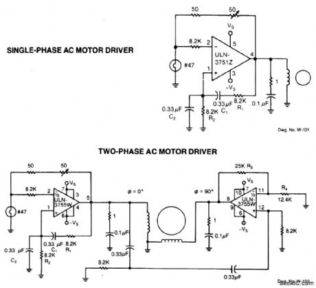
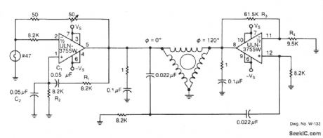
Because of its high amplification factor and built-in power-output stage, an integrated power operational amplifter makes a convenient driver for ac motors. One op amp can be configured as an oscillator to generate the required ac signal. The power-output stage, of course, supplies the high-current drive to the motor. The controlling op amp is configured as a Wein bridge oscillator. The R1C1, R2C2 feedback networks determine the oscillation frequency, according to the following expression:
By varying either R1 or R2, the oscillator frequency can be adjusted over a narrow range.The R3/R4 ratio sets the second amplifier's gain to compensate for signal attenuation occurring in the phase shifters. The circuits can be driven from an external source, such as a pulse or square wave, setting the gain of the left-hand amplifier to a level less than that required for oscillation. The RC feedback networks then function as an active ftlter causing the outputs to be sinusoidal. (View)
View full Circuit Diagram | Comments | Reading(892)
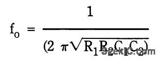
160_METER_BANDPASS
Published:2009/7/3 3:43:00 Author:May
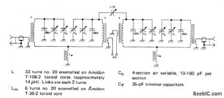
Four-resonator filter is tunable from 1.8 to 2 MHz and has insertion loss of 5 dB.3-dB bandwidth is 30 kHz,and 6-60 dB shape factor is 4.78.Stopband attenuation is over 120 dB.Key to high performance is ward,Bandpass Filters for Receiver Preselecconstruction,and adjustment.-W. Hayward,Bandpass Filter for Receiver Preselectors,Ham Radio,Feb,1975,p 18-27. (View)
View full Circuit Diagram | Comments | Reading(961)
Sine_wave_output_V_F_converter
Published:2009/7/23 23:38:00 Author:Jessie
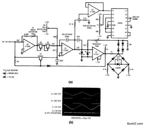
Fig. 12-12 Most of the V/F converters in this chapter produce pulse or square-wave outputs. Many applications (such as audio, filter, or automatic-equipment testing) require a sine-wave output, such as is produced by this circuit. The sine waves from this circuit span a range from 1 Hz to 100 kHz (100 dB or X5 decades) for a 0- to 10-V input, with 0.1% frequency linearity and 0.2% distortion. Drift is 150 ppm/℃ and zero-point drift is 0. 1 Hz/℃. To trim, apply 10.00 V and adjust the 2-kΩ 100-kHz distortion trim for a symmetrical triangle output at Al. Next, apply 100μV and adjust the 50-kΩ 10-Hz distortion trim for triangle symmetry. Then, apply 10.00 V again and adjust the 5-kΩ frequency trim for a 100.00-kHz output. Finally, adjust both 1-kΩ fine distortion trim potentiometers for minimum distortion of the sine-wave output (trace D of Fig. 12-12B). Slight readjustment of the other trim controls might be required to get the lowest possible distortion. (View)
View full Circuit Diagram | Comments | Reading(875)
CAR_WIPER_CONTROL
Published:2009/7/3 3:42:00 Author:May
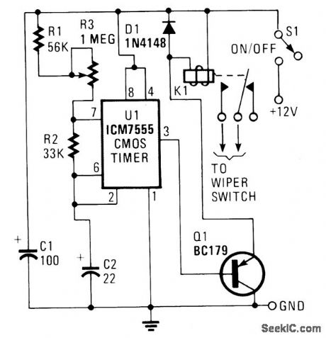
U1 is configured to operate in the standard astable mode, providing a form of relaxation oscillator. When power is applied, C2 initially charges through R1, R2 and R3 to two-thirds of the supply voltage. At that point, U1 senses that its threshold volt-age at pin 6 has been reached, and triggers the timer, causing its output at pin 3 to go high. That high, applied to the base of Q1, keeps the transistor in the off state. Now 02 begins to discharge through R2 to pin 7 of U1. When C2 has discharged to about one-third of the supply voltage, U1 is toggled back to its original state. C2 starts to charge again, as pin 3 of U1 goes low. The low at pin 3 causes Q1-which serves as an emitter-follower buffer stage-to turn on, allowing current to flow through the coil of relay K1. That, in turn, causes K1's contacts to close, applying power to the wipers. The charge time of capacitor C2 is determined by the setting of potentiometer R3. Capacitor C2 should be a tantalum type, and actually, almost any 12-volt coil relay with sufficiently heavy contacts should serve well. (View)
View full Circuit Diagram | Comments | Reading(785)
NARROW_BAND_DEMODULATOR_
Published:2009/7/3 3:42:00 Author:May
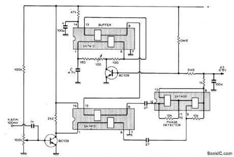
Low-cost TTL ICs are connected to form phase-locked Ioop narrow-band FM demodulator. With value shown for C, circuit is suitable for IF value around 470 kHz. Article covers advantages of synchronous detection and various direct conversion techniques involving phase-locked loop.-P. Hawker、 synchronous Detection in Radio Reception, Wireless World, Nov.1972,p 525-528 (View)
View full Circuit Diagram | Comments | Reading(702)
Alternate_amplifier_with_±120_V_output
Published:2009/7/23 23:37:00 Author:Jessie
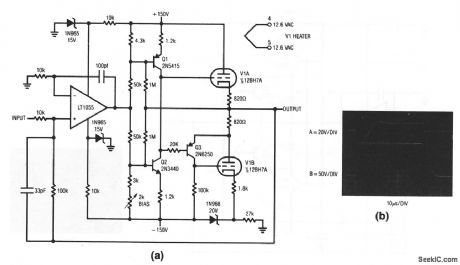
This circuit is similar to that of Fig .1-13, except that vacuum tubes (yes, they still exist ) are used at the output .The full-power band width is 12-kHz with a slew rate of about 12V/μs ,Figure 1-14B shows the results with a ±12-V input (trace A).Danger! this circuit involves high voltages! (View)
View full Circuit Diagram | Comments | Reading(911)
BANDPASS_FOR_CW
Published:2009/7/3 3:42:00 Author:May

Provides bandwidth of about 400 Hz (3 dB down) centered on 875 Hz, for improving reception of CW signals with amateur receiver. Uses three 44-mH toroids.-D. C.Rife, Low-Loss Passive Bandpass CW Filters, QST, Sept. 1971, p 42-44. (View)
View full Circuit Diagram | Comments | Reading(0)
| Pages:1116/2234 At 2011011102110311041105110611071108110911101111111211131114111511161117111811191120Under 20 |
Circuit Categories
power supply circuit
Amplifier Circuit
Basic Circuit
LED and Light Circuit
Sensor Circuit
Signal Processing
Electrical Equipment Circuit
Control Circuit
Remote Control Circuit
A/D-D/A Converter Circuit
Audio Circuit
Measuring and Test Circuit
Communication Circuit
Computer-Related Circuit
555 Circuit
Automotive Circuit
Repairing Circuit