
Circuit Diagram
Index 1201
Low_distortion_oscillator
Published:2009/7/24 9:01:00 Author:Jessie
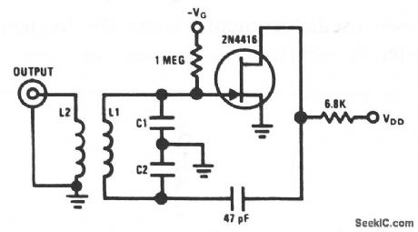
The 2N4416 JFET is capable of oscillating in a circuit, where harmonic distortion is very low. The JFET oscillator is excellent when a low harmonic content is required for a good mixer circuit. The values given are for a 20-MHz oscillator. National Semiconductor, Linear Applications Handbook, 1991, p. 114. (View)
View full Circuit Diagram | Comments | Reading(1)
Stable_low_frequency_crystal_oscillator
Published:2009/7/24 9:00:00 Author:Jessie
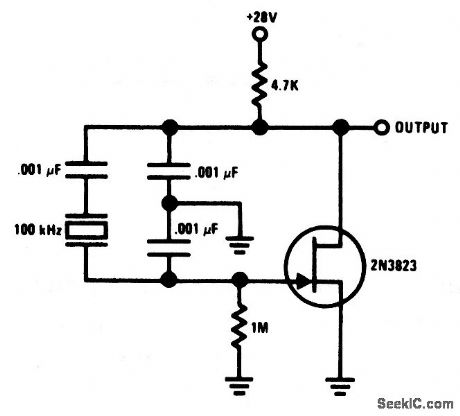
This Colpitts crystal oscillator is ideal for low-frequency oscillator applications. Excellent stability is assured because the 2N3823 JFET circuit loading does not vary with temperature. National Semiconductor, Linear Applications Handbook, 1991, p. 114. (View)
View full Circuit Diagram | Comments | Reading(1150)
LOW_POWER_BINARY_TO_10SUPn_SUP_GAIN_LOW_FREQUENCY_AMPLIFIER
Published:2009/7/1 1:55:00 Author:May
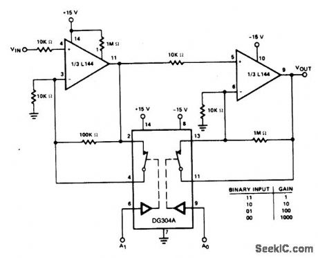
Gain increases by decades as the binary input decreases from 1,1 to 0,0. Minimum gain is 1 and maximum gain is 1000, Since the switch is static in this type of amplifier the power dissipation of the switch will be less than a tenth of a milliwatt. (View)
View full Circuit Diagram | Comments | Reading(627)
JFET_Pierce_crystal_oscillator
Published:2009/7/24 8:59:00 Author:Jessie
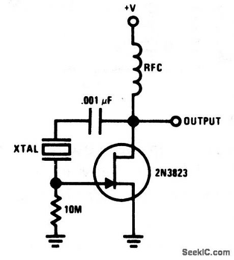
This circuit allows a wide frequency range of crystals to be used without circuit modification. Because the JFET gate does not load the crystal, good Q is maintained, which thus ensures good frequency stability. National Semiconductor, Linear Applications Handbook, 1991, p. 106. (View)
View full Circuit Diagram | Comments | Reading(910)
LOW_POWER_INVERTING_AMPLIFIER_WITH_DIGITALLY_SELECTABLE_GAIN
Published:2009/7/1 1:55:00 Author:May

View full Circuit Diagram | Comments | Reading(788)
Temperature_compensated_crystal_oscillator
Published:2009/7/24 8:27:00 Author:Jessie
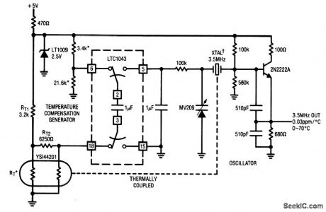
This circuit uses an LTC1043 to differentiate between a temperature-sensing network and a dc reference. The singla-ended output biases a varactortuned crystal oscillator to compensate drift. The varactor-crystal network has high dc impedance, with eliminates the need for an output amplifier from the LTC1043. Connect other LTC1043 pins as follows: 4 to +5 V, 16 to ground through a 0.001-μF capacitor, and 17 directly to ground. Linear Technology, Linear Applications Handbook, 1990, p. AN3-15. (View)
View full Circuit Diagram | Comments | Reading(2235)
PHOTODIODE_CURRENT_TO_VOLTAGE_CONVERTER
Published:2009/7/1 1:53:00 Author:May
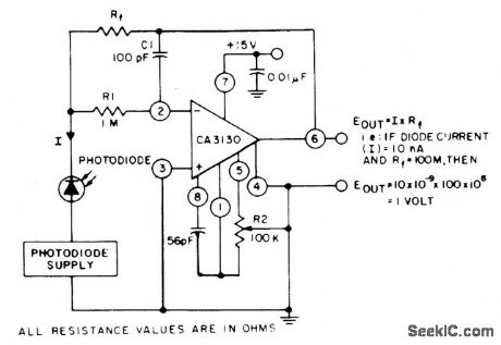
The circuit uses three CA3130 BiMOS op amps in an application sensitive to sub-picoampere input currents. The circuit provides a ground-referenced output voltage proportional to input current flowing through the photodiode. (View)
View full Circuit Diagram | Comments | Reading(1540)
Basic_positive_buck_converter
Published:2009/7/24 8:26:00 Author:Jessie
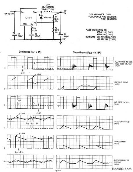
This circuit is used to convert a larger positive input voltage to a lower positive output, using an LT1074 switching regulator. Typical waveforms are shown in Fig. 4-39B. These waveforms are based on a VIN of 20 V, VOUT of 5 V, and L of 50μH for both continuous mode (inductor current never drops to zero) with IOUT of 3A, and discontinuous mode (inductor current drops to zero during a potion of the switching cycle (IOUT =0.17 A). (View)
View full Circuit Diagram | Comments | Reading(809)
THERMALLY_STABILIZED_PPIN_PHOTODIODE_SIGNAL_CONDITIONER
Published:2009/7/1 1:50:00 Author:May
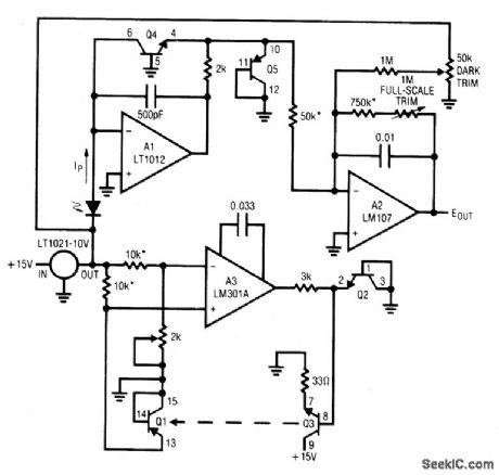
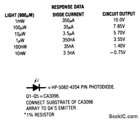
The photodiode specified responds linearly to light intensity over a 100 dB range.Digitizing the diodes linearly amplified output would require an A-D converter with 17 bits of range. This requirement can be eliminated by logarithmically compressing the diode's output in the signal conditioning circuity. Al and Q4 convert the diode's photocurrent to voltage output with a logarithmic transfer function. A2 provides offsetting and additional gain. A3 and its associated components form a temperature control loop
which maintains Q4 at constant temperature (all transistors in this circuit are part of a CA3096 monolithic array). The 0.033μF value at A3's compensation pins gives good loop damping if the circuit is built using the array's transistors in the location shown.
Because of the array de's small size, response is quick and clean. A full-scale step requires only 250 ms to settle to final value. To use this circuit, first set the thermal control loop.To do this, ground Q3's base and set the 2 k pot so A3's negative input voltage is 55 mV above its positive input. This places the servo's setpoint at about 50℃(25℃ ambient + (2.2 mV/℃, x 25℃ rise = 55 mV = 50℃). Unground Q3's base and the array will come to temperature. Next, place the photodiode in a completely dark environment and adjust the dark trim so A2's output is 0 V. Finally, apply or electrically simulate 1 mW of light and set the full-scale trim for 10 V out. Once adjusted, this circuit responds logarithmically to light inputs from 10nW to 1mW with an accuracy limited by the diode's 1% error.
(View)
View full Circuit Diagram | Comments | Reading(797)
HIGH_IMPEDANCE_LOW_CAPACITANCE_AMPLIFIER
Published:2009/7/1 1:50:00 Author:May
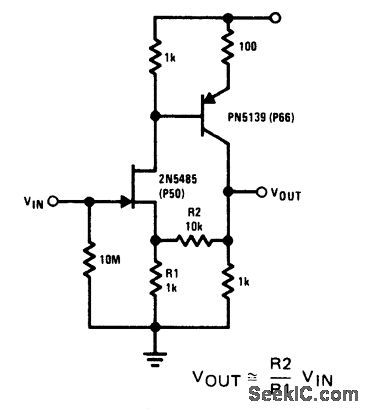
This compound series-feedback circuit provides high input impedance and stable,wide-band galn for general purpose video amplifier applications. (View)
View full Circuit Diagram | Comments | Reading(985)
FET_CASCODE_VIDEO_AMPLIFIER
Published:2009/7/1 1:49:00 Author:May
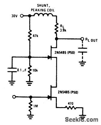
The FET cascode video amplifier features very low input loading and reduction of feed-back to almost zero. The 2N5485 is used be-cause of its low capacitance and high Yfs. Bandwidth of this amplifier is limited by R1, and load capacitance. (View)
View full Circuit Diagram | Comments | Reading(2095)
MONOSTABLE_PHOTOCELL_CIRCUIT_HAS_SELF_ADJUSTING_TRIGGER_LEVEL
Published:2009/7/1 1:49:00 Author:May
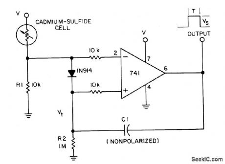
A photocell circuit provides automatic threshold adjustment. Monostable actionprevents undesired retriggering of the output. With only one op amp IC,the circuit offers:Automatic adjustment of its trigger level to accommodate vanous light Sources,changesh ambient light and misalignments;A built-in monostable action to provide only a singleoutput pulse during a preset time;Feedback action toralse the threshold level aftertriggering and to speed switching.The feedback also eliminates the circuit's tendencyto oscillate during switching (View)
View full Circuit Diagram | Comments | Reading(2182)
PRECISION_PEAK_TO_PEAK_AC_DC_CONVERTER
Published:2009/7/1 1:48:00 Author:May
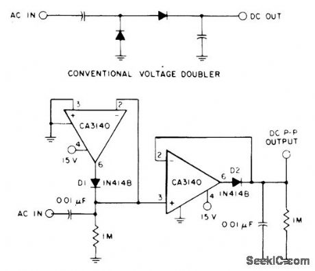
Using a CA3140 BiMOS op amp and a single positive supply converts a conventional voltage doubler with two precision diodes into a precision peak-to-peak ac-to-dc voltage converter having wide dynamic range and wide bandwidth. (View)
View full Circuit Diagram | Comments | Reading(2364)
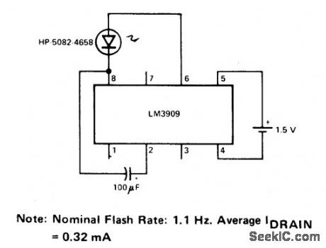
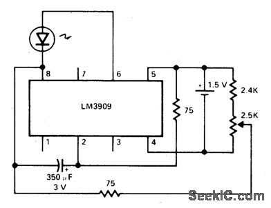
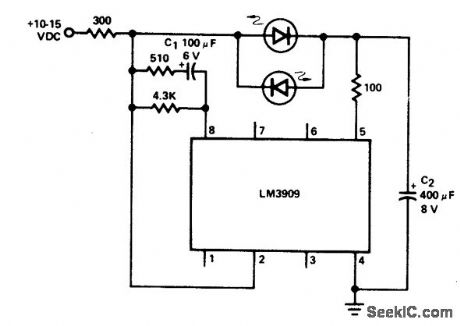
MINIMUM_POWER_FLASHER(15_V)
Published:2009/7/1 1:48:00 Author:May
View full Circuit Diagram | Comments | Reading(706)
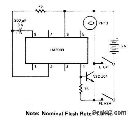
EMERGENCY_LANTERN/FLASHER_
Published:2009/7/1 1:47:00 Author:May
View full Circuit Diagram | Comments | Reading(778)
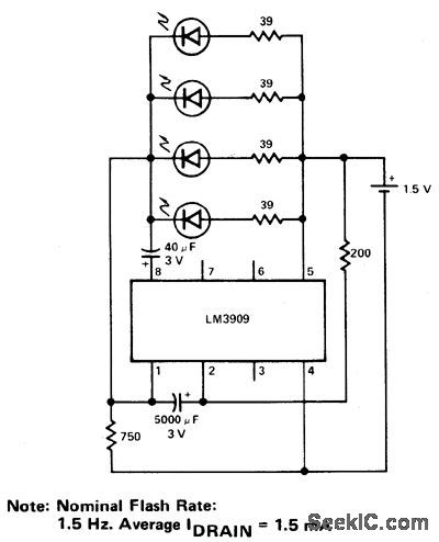
HIGH_EFFICIENCY__PARALLEL_CIRCUIT_FLASHER_
Published:2009/7/1 1:46:00 Author:May
View full Circuit Diagram | Comments | Reading(834)
FREQUENCY_DIVIDER
Published:2009/7/1 1:46:00 Author:May
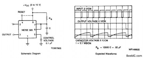
If the input frequency is known, the timer can easily be used as a frequency divider by adjusting the length of the timeing cycle. Figure shows the waveforms of the timer when used as a divide-by-three circuit. This application makes use of the fact that this circuit cannot be retriggered during the timing cycle. (View)
View full Circuit Diagram | Comments | Reading(2222)
VARIABLE_FLASHER_
Published:2009/7/1 1:46:00 Author:May
View full Circuit Diagram | Comments | Reading(701)
MODULATED_LIGHT_BEAM_CIRCUIT_CANCELS_AMBIENT_LIGHT_EFFECTS
Published:2009/7/1 1:46:00 Author:May
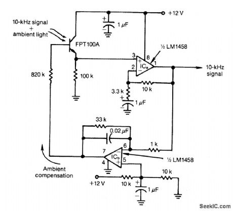
Feedback control of the phototransistor in this optical detector helps negate the effects of varying ambient light sources. The output of a modulated visible-light LED is detected, amplified, buffered, and fed through a low-pass ftlter. Ambient light signals below the LED's 10-kHz modulating rate reach the detector's base out of phase with incoming ambient light and cancel the undesired effects. (View)
View full Circuit Diagram | Comments | Reading(1157)
ALTERNATING_FLASHER
Published:2009/7/1 1:44:00 Author:May
View full Circuit Diagram | Comments | Reading(0)
| Pages:1201/2234 At 2012011202120312041205120612071208120912101211121212131214121512161217121812191220Under 20 |
Circuit Categories
power supply circuit
Amplifier Circuit
Basic Circuit
LED and Light Circuit
Sensor Circuit
Signal Processing
Electrical Equipment Circuit
Control Circuit
Remote Control Circuit
A/D-D/A Converter Circuit
Audio Circuit
Measuring and Test Circuit
Communication Circuit
Computer-Related Circuit
555 Circuit
Automotive Circuit
Repairing Circuit