
Circuit Diagram
Index 1200
0_V_TO_20_V_POWER_REFERENCE
Published:2009/7/1 2:01:00 Author:May
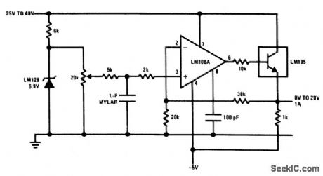
View full Circuit Diagram | Comments | Reading(566)
Adjustable_dc_dc_step_up_converter15_A
Published:2009/7/25 1:15:00 Author:Jessie

This circuit shows an LAS-6350/6450 used as a step-up converter with an adjustable output. (View)
View full Circuit Diagram | Comments | Reading(741)
1_A_dc_dc_step_down_converter_
Published:2009/7/25 0:27:00 Author:Jessie


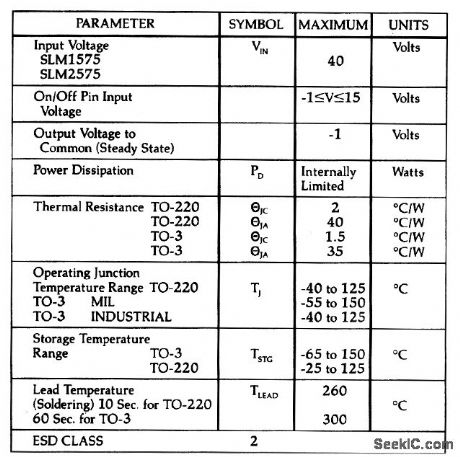
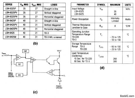
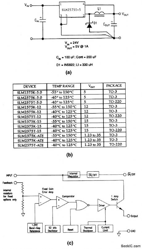
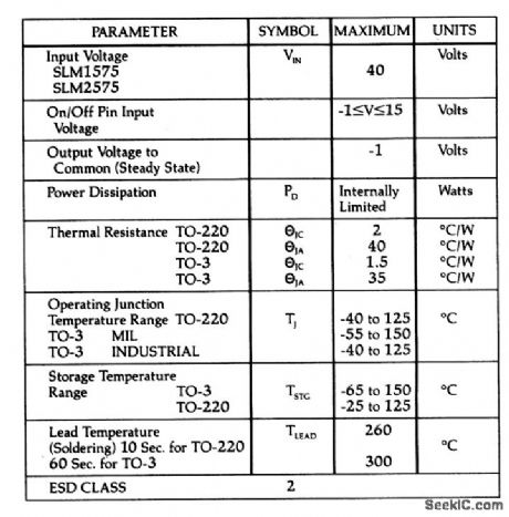
The SLM switching-regulator ICs contain most elements necessary for converter operation, as shown in Fig. 4-2C. Figure 4-2B shows the output voltage and characteristics for various part numbers. Figure 4-2D shows the absolute maximum ratings. Simply add a choke, catch diode, and two capacitors to the IC for a complete converter. (View)
View full Circuit Diagram | Comments | Reading(661)
100_MHz_CONVERTER
Published:2009/7/1 2:01:00 Author:May
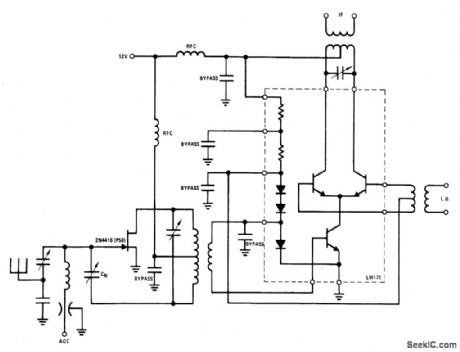
The 2N4416 JFET will provide noise figures of less than 3 dB and power gain of greater than 20 dB. The JFET's outstanding low crossmodulation and low intermodulation distortion provides an ideal characteristic for an input stage. The output feeds into an LM171 used as a balanced mixer. This configuration greatly reduces local oscillator radiation both into the antenna and into the if strip and also reduces rf signal feedthrough. (View)
View full Circuit Diagram | Comments | Reading(1041)
Timer_multivibrator
Published:2009/7/25 Author:Jessie
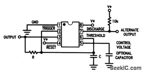
This circuit shows a general-purpose ICM7555/56 timer connected as a free-running multivibrator, with a true 50% duty-cycle output. The frequency is determined by 1.44/RC, with a maximum of about 1 MHz. Use high values of R and low values of C for minimum current drain. At a supply of 4.5 V, the circuit will drive at least two TTL loads. (View)
View full Circuit Diagram | Comments | Reading(736)
BILATERAL_CURRENT_SOURCE
Published:2009/7/1 2:00:00 Author:May
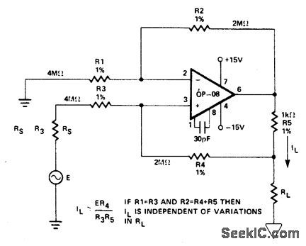
The circuit will produce the current re-lationship to within 2% using 1% values for R1 through R5. This includes variations in RL from 100 ohm to 2000 ohm. The use of large resis-tors for R1 through R4 minimizes the error due to Rt variations. The large resistors are possi-ble because of the excellent input bias current performance of the OP-08. (View)
View full Circuit Diagram | Comments | Reading(0)
LVDT_DRIVER_DEMODULATOR
Published:2009/7/1 1:59:00 Author:May
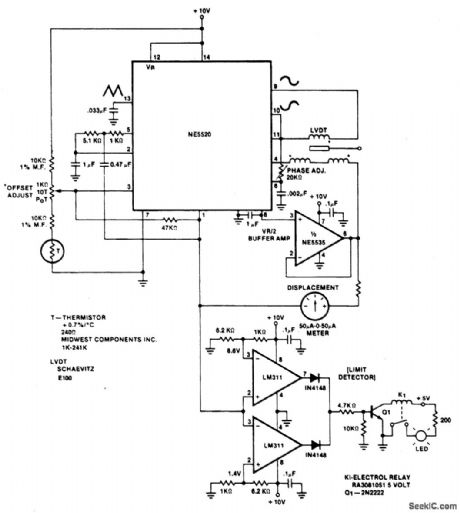
View full Circuit Diagram | Comments | Reading(1478)
VIDEO_AMPLIFIER_2
Published:2009/7/1 1:58:00 Author:May
View full Circuit Diagram | Comments | Reading(1347)
FREQUENCY_TO_VOLTAGE_CONVERTERS
Published:2009/7/1 1:58:00 Author:May
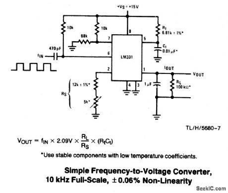
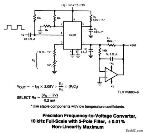
In these applications, a pulse input at fIN is differentiated by a C-R network and the negative-going edge at pin 6 causes the input comparator to trigger the timer circuit.Just as with a V-to-F converter, the average current flowing out of pin 1 is IAVERAGE = i x (1.1 R1C1) x f. In this simple circuit, this current is filtered in the network Rt = 100 k ohm and 1 μF. The ripple will be less than 10 mV peak, but the response will be slow, with a 0.1 second time constant, and settling of 0.7 second to 0.1% accuracy.In the precision circuit,an operatiot amplifier provides a buffered outputand also acts as a 2-pole filter.The ripple will be less than 5 mV peak forall frequenciesabove 1 kHz,and the response time will be much quicker than in Part 1,However,for input frequencies below 200 Hz,this circuit will have worse ripple than the figure。The engineering of the filter time-constants to get adequate response and small enough ripple simply requlres a study of the compromises to be made.Inherently V-to-Fconverter response can be fast, but F-to-Ⅴ response cannot. (View)
View full Circuit Diagram | Comments | Reading(1181)
RMS_TO_DC_CONVERTER
Published:2009/7/1 1:58:00 Author:May
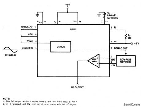
An ac voltmeter may be easily constructed. Simplicity of the circuit and low component count make it particularly attractive. The demodulator output is a full-wave rectified signal from the ac input at Pin 4. The dc component on the rectified signal at Pin 5 varies linearity with the rms input at Pin 4 and thus provides an accurate rms-to-dc conversion at the output of the filter (Pin 1). CT is a variable capacitor that is tweaked until the oscillator signal to the sync input of the demodulator is in phase with the ac signal at Pin 4. (View)
View full Circuit Diagram | Comments | Reading(1281)
OTA_gain_control_amplifier
Published:2009/7/24 23:59:00 Author:Jessie
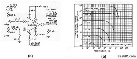
This circuit shows an OTA in a typical gain-control amplifier application. Figure 11-5B shows some typical characteristics. With an IABC of 1 mA,the gm is about 16 mmhos. With the CA3280 operating into a 5-KΩ resistor,the gain is 80. (View)
View full Circuit Diagram | Comments | Reading(823)
VIDEO_AMPLIFIER
Published:2009/7/1 1:58:00 Author:May
View full Circuit Diagram | Comments | Reading(0)
Basic_square_root_circuit
Published:2009/7/24 23:59:00 Author:Jessie
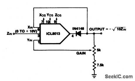
This circuit shows an ICL8013 (refer to Fig. 3-15) connected as a basic square root circuit. Use the following trim procedure.1. Connect the ICL8013 in the divider configuration (Fig. 3-16). 2. Adjust Zos, Yos, Xos, and gain using steps 1 through 6 of the divider trim procedure.3. Convert to the square-root configuration by connecting XIN to the output and inserting a diode between pin 4 and the output, as shown in Fig. 3-18.4. With ZIN =0 V adjust Zos for zero output voltage.
.
(View)
View full Circuit Diagram | Comments | Reading(782)
A_PRECISION_AMPLIFIER_WITH_DIGITALLY_PROGRAMMABLE_INPUTS_AND_GAIN
Published:2009/7/1 1:58:00 Author:May
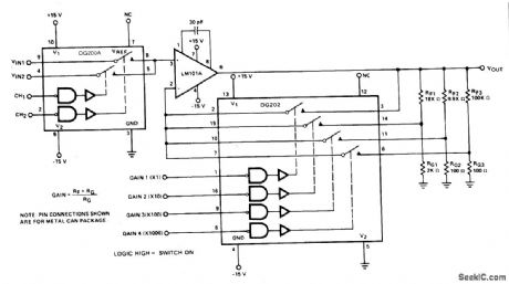
View full Circuit Diagram | Comments | Reading(623)
OTA_sample_hold_circuit
Published:2009/7/24 23:58:00 Author:Jessie
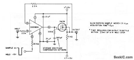
This circuit shows one section of an OTA combined with a JFET to form a sample-hold configuration. (View)
View full Circuit Diagram | Comments | Reading(848)
PROGRAMMABLE_AMPLIFIER
Published:2009/7/1 1:57:00 Author:May
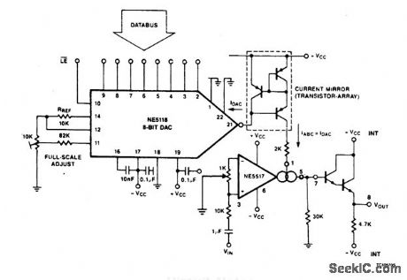
The intention of the following application shows how the NE5517 works in connection with a DAC. In the application, the NE5118 is used-an 8-bit DAC with current output-its input register making this device fully μP-compatible. The circuit consists of three functional blocks; the NE5118 which generates a control current equivalent to the applied data byte, a current mirror, and the NE5517. (View)
View full Circuit Diagram | Comments | Reading(1541)
JFET_BIPOLAR_CASCODE_VIDEO_AMPLIFIER
Published:2009/7/1 1:57:00 Author:May

The JFET-bipolar cascade circuit will provide full video output for the CRT cathode drive. Gain is about 90. The cascode configura-tion e liminate s Millercapacitance problems with the 2N4091 JFET, thus allowing direct drive from the video detector. An m-derived filter using stray capacitance and a variable inductor prevents 4.5 MHz sound frequency from being amplified by the video amplifier. (View)
View full Circuit Diagram | Comments | Reading(1695)
Digital_memory_backup_for_SRAMs
Published:2009/7/24 12:26:00 Author:Jessie
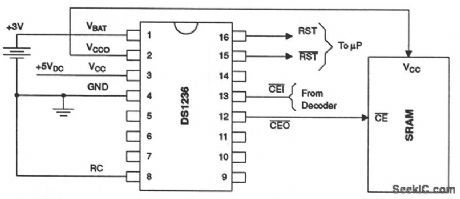
This circuit shows a DS1236 that is used to control battery-backup operation for a static RAM. First, the DS1236 contains a switch to direct SRAM power from the 5-V supply (VCC) or from an external battery (VBAT), whichever is greater. The switched supply (VCCO) can also be used to battery-back a CMOS processor. Second, the same power-fail detection (using RST and RST ) that is described for the digital power monitor (Fig. 6-53) is used to hold the chip-enable output (CEO ) to within 0.3 V of VCC or to within 0.7 V of VBAT. This write-protection mechanism occurs as VCC falls below a specified trip point, VCCTP. Dallas Semiconductors, Product Data Book, 1992/1993, p. 10-74. (View)
View full Circuit Diagram | Comments | Reading(2384)
LOW_POWER_NON_INVERTING_AMPLIFIER_WITH_DIGITALLY_SELECTABLE_INPUTS_AND_GAIN
Published:2009/7/1 1:56:00 Author:May
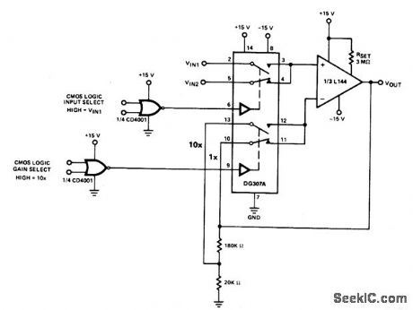
View full Circuit Diagram | Comments | Reading(709)
SELF_OSCILLATING_FLYBACK_CONVERTER
Published:2009/7/1 1:56:00 Author:May
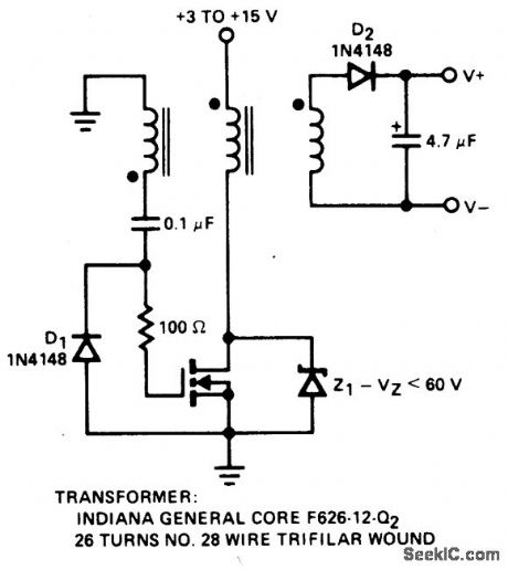
Low-power converter uses the core characteristics to determine frequency. With the transformer shown, operating frequency is 250 kHz. Diode D1prevents negative spikes from occurring at the MOSFET gate, the 100 ohm resistor is a parasitic suppressor, and Z1 serves as a dissipative voltage regulator for the output and also cUps the drain voltage to a level below the rated power FET breakdown voltage. (View)
View full Circuit Diagram | Comments | Reading(0)
| Pages:1200/2234 At 2011811182118311841185118611871188118911901191119211931194119511961197119811991200Under 20 |
Circuit Categories
power supply circuit
Amplifier Circuit
Basic Circuit
LED and Light Circuit
Sensor Circuit
Signal Processing
Electrical Equipment Circuit
Control Circuit
Remote Control Circuit
A/D-D/A Converter Circuit
Audio Circuit
Measuring and Test Circuit
Communication Circuit
Computer-Related Circuit
555 Circuit
Automotive Circuit
Repairing Circuit