
Circuit Diagram
Index 1182
AMMETER_WITH_SIX_DECADE_RANGE
Published:2009/7/1 4:29:00 Author:May
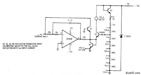
The Ammeter measures currents from 100 pA to 100 μA without the use of expensive high value resistors. Accuracy at 100μA is limited by the offset voltage between Q1 and Q2 and, at 100 pA, by the inverting bias current of the LT1008. (View)
View full Circuit Diagram | Comments | Reading(811)
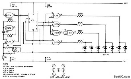
ELECTRONIC_DICE
Published:2009/7/1 4:28:00 Author:May


Circuit Notes
Six LEDs are arranged to produce a dis-play the same as the dots on a dice. When PBI is depressed, the display is blanked and the os-cillator (IC1| a, b, c) clocks IC2 at about 1MHz.IC2 counts from zero and resets on seven. When PBI is released, the display is enabled and a decoding system (IC3) produces the cor-rect output on the LEDs. (View)
View full Circuit Diagram | Comments | Reading(2359)
VOLTAGE_CONTROLLED_ATTENUATOR
Published:2009/7/1 4:27:00 Author:May
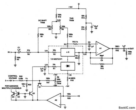
Op amp A2 and transistors Q1 and Q2 form the exponential converter generating an exponential gain control current, which is fed into the rectifier.A reference current of 150 μA, (15 V and R20=100 k), is attenuated a factor of two (6 dB) for every volt increase in the control voltage. Capacitor C6 slows down gain changes to a 20 ms time constant (C6 x R1) so that an abrupt change in the control voltage will produce a smooth sounding gain change. R18 ensures that for large control voltages the circuit will go to full attentudtion. The rectifier bias current would normally limit the gain reduction to about 70 dB. R16 draws excess current out of the rectifier. After approximately 50 dB of attentuation at a -6 dB/V slope, the slope steepens and attenuation becomes much more rapid until the circuit totally shuts off at about 9 V of control voltage. A1 should be a low-noise high slew rate op amp. R13 and R14 establish approximately a 0 V bias at A1's output. (View)
View full Circuit Diagram | Comments | Reading(2506)
GUARDED_INPUT_PICOAMMETER_CIRCUIT
Published:2009/7/1 4:26:00 Author:May
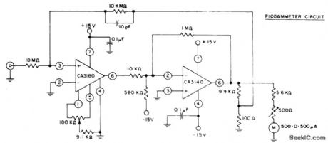
The circuit utilizes CA3160 and CA3140 BiMOS op amps to provide a full-scale meter deflection of ±3 pA. The CA3140 serves as an X100 gain stage to provide the required plus and minus output swing for the meter and feedback network. Terminals 2 and 4 of the CA3160 are at ground potential, thus its input is operated in the guarded mode. (View)
View full Circuit Diagram | Comments | Reading(2153)
OPERATIONAL_AMPLIFIER_CONTROL
Published:2009/7/24 3:55:00 Author:Jessie
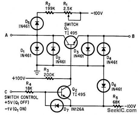
Switch must pass 1 ma in either direction (A to B or B to A). Diode pairs D1-D2 and D3-D4 are voltage limiters, while Q1 is basic switching element. Switching time is about 2 microsec.Used as sample-and-hold circuit, with 500-microsec sampling interval-R. W. Maloy, Transistor Switch Passes Current Both Ways, Electronics, 38:1, p 79. (View)
View full Circuit Diagram | Comments | Reading(848)
AUDIO_AUTOMATIC_GAIN_CONTROL
Published:2009/7/1 4:24:00 Author:May
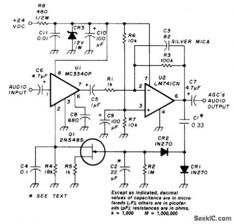
An audio signal applied to U1 is passed through to the 741 operational amplifier, U2. After being amplified, the output signal of U2 is sampled and applied to a negative voltage doubler/rectifier circuit composed of diodes CR1 and CR2 along with capacitor C1. The resulting negative voltage is used as a control voltage that is applied to the gate of the 2N5485 JFET Q1. Capacitor C2 and resistor R2 form a smoothing filter for the rectified audio control voltage.The JFET is connected from pin 2 of the MC3340P to ground through a 1 kilohm resistor. As the voltage applied to the gate of the JFET becomes more negative in, magnitude, the channel resistance of the JFET increases causing the JFET to operate as a voltage controlled resistor. The MC3340P audio attenuator is the heart of the AGC. It is capable of 13 dB gain or nearly -80 dB of attenuation depending on the external resistance placed between pin 2 and ground. An increase of resistance decreases the gain achieved through the MC3340P. The circuit gain is not entirely a linear function of the external resistance but approximates such behavior over a good portion of the gain/attenuation range. An input signal applied to the AGC input will cause the gate volt-age of the JFET to become proportionally negative. As a result the JFET increases the resistance from pin 2 to ground of the MC3340P causing a reduction in gain. In this way the AGC output is held at a nearly constant level. (View)
View full Circuit Diagram | Comments | Reading(1692)
ELECTROMETER_AMPLIFIER_WITH_OVERLOAD_PROTECTION
Published:2009/7/1 4:22:00 Author:May
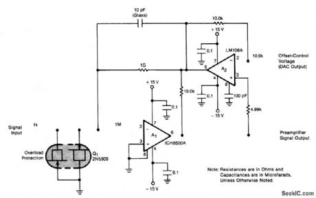
The preamplifier is protected from excessive input signals of either polarity by the 2N5909 junction field-effect transistor. A nulling circuit makes it possible to set the preamplifier output voltage to zero at a ftxed low level (up to ±10-8A) of the input current. (This level is called the standing current and corresponds to the zero-signal level of the instrumentation.) The opposing (offset) current is generated in the 109 feedback resistor to buck the standing current. Different current ranges are reached by feeding the preamplifter output to low and high gain amplifter chains. To reduce noise, each chain includes a 1.5 Hz corner active filter. (View)
View full Circuit Diagram | Comments | Reading(1433)
33_V_5_V_5_V_step_up_converter
Published:2009/7/24 3:54:00 Author:Jessie
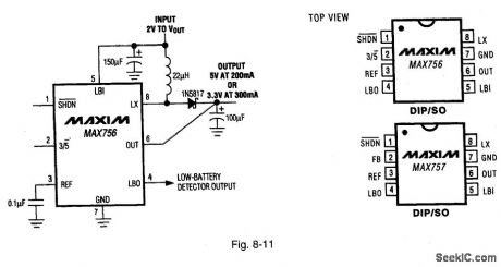
Figure 8-11 shows a MAX756 connected to provide a 5-V output at 200 mA or 3.3 V at 300 mA(depending on the status of 3/5 pm 2)with an input from 1.1 V to 5.5 V Quiescent current is 60 μA with a 20-μA shutdown current, and an efficiency of 87% (at 200 mA).MAXIM NEW RELEASES DATA Book 1994. P. 4-173.
(View)
View full Circuit Diagram | Comments | Reading(682)
HIGH_CURRENT_HIGH_SPEED_SWITCH
Published:2009/7/24 3:54:00 Author:Jessie

Alloy junction transistor (2N2648 germanium) has useful frequency range up to 10 Mc for switching up to 1 amp with gain of 50 in 0.8 microsec.-Medium Power Transistor Has Multiple Uses, Electronics, 361, p 132. (View)
View full Circuit Diagram | Comments | Reading(1024)
SPEAKER_OVERLOAD_PROTECTOR
Published:2009/7/1 4:22:00 Author:May
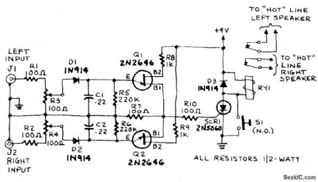
The input to the circuit is taken from the amplifier's speaker-output terminals or jacks. If the right-channel signal is sufficiently large to charge C1 to a potential that is greater than the breakdown voltage of Q1's emitter, a voltage pulse will appear across R7. Similarly, if the left-channel signal is sufftciently large to charge C2 to a potential that is greater than the breakdown voltage of Q2's emitter, a pulse will appear across R7. The pulse across R7 triggers SCR1, a sensitive gate SCR (IGT less than 15 mA where IGT is the gate trigger-current), that latches in a conducting state and energizes RY1. The action of the relay will interrupt both speaker circuits, and the resulting silence should alert you to the problem. Cut back the volume on your amplifier, then press and release S1 to reset the circuit and restore normal operation. The circuit can be adjusted to trip at any level from 15 to 150 watts RMS. To calibrate, deliberately feed an excessive signal to the right input of the speaker protector and adjust R3 until RY1 energizes. Do the same with the left channel, this time adjusting R4. The circuit is now calibrated and ready for use. (View)
View full Circuit Diagram | Comments | Reading(1324)
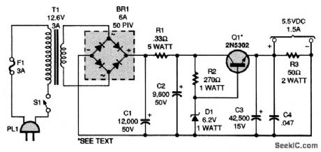
IR_TRANSMITTER_POWER_SUPPLY
Published:2009/7/24 3:54:00 Author:Jessie
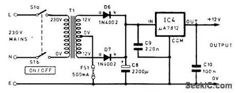
This supply provides 12 Vdc for an IR transmitter or other circuit. The current is about 260 mA. A 120-V transformer can be substituted for the 230-V unit shown, if desired. (View)
View full Circuit Diagram | Comments | Reading(583)
SCS_CONTACT_ISOLATOR
Published:2009/7/24 3:53:00 Author:Jessie
Eliminates contact bounce in grounded-switch arrangement where switch is opened to trigger scs.- transistor Manual, Seventh Edition, General Electric Co., 1964, p 433. (View)
View full Circuit Diagram | Comments | Reading(613)
16__to_30_MHz_100__140__180_W_linear_amplifier_for_mobile_operation
Published:2009/7/24 3:53:00 Author:Jessie
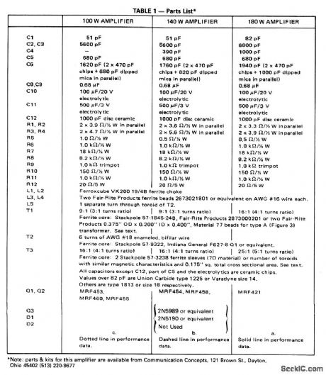
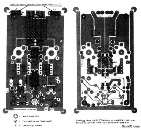
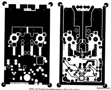
Figure 2-54A shows the basic circuit for the amplifier, and Fig.2-54B shows the parts list for three verslons of the circuit. All three verslons operate with a 13.6-V supply. The component layout,and PC-board layout,are shown in Figs.,2-54C and 2-54D,respectively.Both the parts and kits for this amplifier are available from∶Communications Concepts.121 Brown St, Dayton, Ohio 45402,(513) 220-9677. (View)
View full Circuit Diagram | Comments | Reading(982)
10_KV_SWITCHING_CIRCUIT
Published:2009/7/24 3:53:00 Author:Jessie
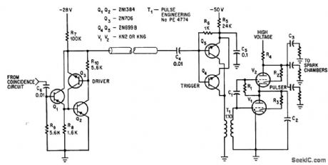
Cold-cathode gas tubes provide reliable switching of high voltage to army of spark chambers in bal-loon-borne equipment. Three-transistor line driver can be to feet away. Negative pulse input to Q1 makes Q2 and Q3 go into regenerative mode, discharging C4 to turn on trigger that applies 500 V to ire pulser.-R. E. Daniels and A. D. Cook, Cold-Cathode Gas Tubes Switch High Voltage Fast, Electronics, 37:14, p 72-73. (View)
View full Circuit Diagram | Comments | Reading(759)
ANTIQUE_RADIO_POWER_SUPPLY
Published:2009/7/24 3:52:00 Author:Jessie
This supply was intended for powering an antique radio using 01A triodes needing dc filament voltage. It is a straightforward zener regulator and pass transistor. The large values or capacitance used are for reducing 120-Hz hum to a minimum. (View)
View full Circuit Diagram | Comments | Reading(899)
Low_voltage_single_cell_step_up_converter
Published:2009/7/24 3:52:00 Author:Jessie
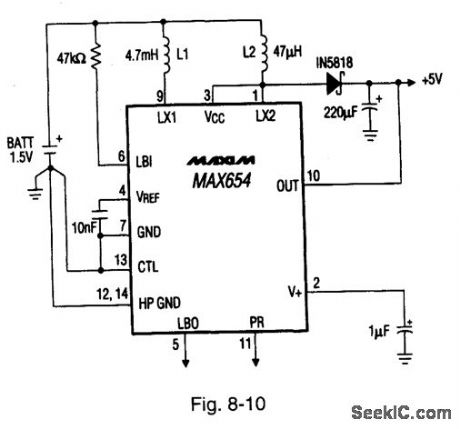
Figure 8-10 shows a MAX654 connected to provide a +5-V output at 40 mA with a 1.5-V input. The guaranteed start-up voltage is 1.15 V. The quiescent current shutdown is 80 μA. MAXIM HIGH RELIABILITY DATA Book, 1993, P. 4-37.
(View)
View full Circuit Diagram | Comments | Reading(641)
THREE_DIODE_SWITCH_FOR_VIDEO_TIME_SHARING
Published:2009/7/24 3:52:00 Author:Jessie
Gate pulse applied to diode D1draws current from R1 through D1 (switch open) or through D2 and D3 (switch closed so video passes from input to output). Clamp diode D4 keeps base line of output always positive.-T. Vagt, New Light on Air Traffic: Bright Plan Display with Alphanumerics, Electronics, 36:30, p 42-46. (View)
View full Circuit Diagram | Comments | Reading(701)
SMART_AC_POWER_STRIP
Published:2009/7/24 3:51:00 Author:Jessie
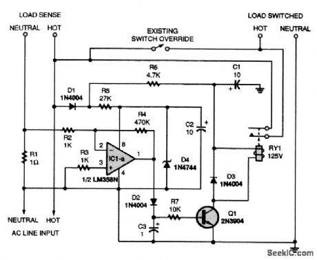
The schematic of the Smart Strip circuit is shown. The ac line input is connected directly to the 117-Vac line of a power strip. The voltage is rectified by diode D1 and filtered by capacitor C2. The load-sense lines are connected to the ac socket in the power strip that will contain the device that will be used to turn the others on. When the load sense device is turned on, current flows through R1, a 1-Ω, 10-W resistor. To limit the power in R1 to 5 W, therefore, amaximum load ofno more than 5 A should be connected to the load sense outlet. The resulting voltage drop across R1 is fed to one section of an LM358N op amp, IC1-a, through resistors R2 and R3. Zener diode D4 limits the supply for the op amp to 15 Vdc. The voltage drop across R1 could be very small if the device plugged into the load sense socket does not draw much current. To ensure that the circuit is sensitive enough to detect such small-load devices, the gain of IC1-a is set at 470 by resistors R2 and R4. Because the out-put IC1-a is halfway rectified, diode D2 and capacitor C3 are used to form a peak-hold circuit. As long as CB is charged to 0.7 V or more (when a powered-up load sense device is detected), transistor Q1 will be on, and relay RY1 will close. When those normally open contacts close, the hot line is connected to the load-switched sockets, effectively turning on any devices that are connected to those outlets. Diode D1, resistor R6, and capacitor C1 provide a dc supply for the 12-V coil of the relay; diode D3 acts as a clamping diode. (View)
View full Circuit Diagram | Comments | Reading(3422)
High_efficiency__5_V_step_dozon_regulator
Published:2009/7/24 3:50:00 Author:Jessie
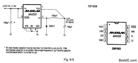
Figure 8-9 shows a MAX639 connected to provide +5-V output at 100 mA with inputs from +5.5 V to +11.5 V. Maximum quiescent current is 20 μA, with a typicai dropout of 0.5 V at (100-mA load). Efficiency is greater than 90%. MAXIM HIGH RELIAsILITY DATA BOOK, 1993, P. 4-31.
(View)
View full Circuit Diagram | Comments | Reading(605)
TWO_TRANSISTOR_PHANIASTRON
Published:2009/7/24 3:50:00 Author:Jessie
Q1 and Q2 simulate vacuum-tube phantastron sweep generator, Since input impedance is low, linearity con be improved by using emitter-follower Q3.-N. C. Hekimian, Phantastron Circuits Using Transistors, Electronics, 34:8, p 46-47. (View)
View full Circuit Diagram | Comments | Reading(791)
| Pages:1182/2234 At 2011811182118311841185118611871188118911901191119211931194119511961197119811991200Under 20 |
Circuit Categories
power supply circuit
Amplifier Circuit
Basic Circuit
LED and Light Circuit
Sensor Circuit
Signal Processing
Electrical Equipment Circuit
Control Circuit
Remote Control Circuit
A/D-D/A Converter Circuit
Audio Circuit
Measuring and Test Circuit
Communication Circuit
Computer-Related Circuit
555 Circuit
Automotive Circuit
Repairing Circuit