
Circuit Diagram
Index 1191
Noninverting_comparator_with_hysteresis
Published:2009/7/24 4:21:00 Author:Jessie
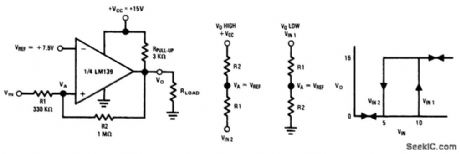
Fig. 15-6 This circuit is similar to that of Fig. 15-5, except that the output is noninverting. National Semiconductor Linear Applications Handbook 1991 p 259. (View)
View full Circuit Diagram | Comments | Reading(0)
FAST_SWITCHING_OF_D_C_POWER
Published:2009/7/24 4:21:00 Author:Jessie
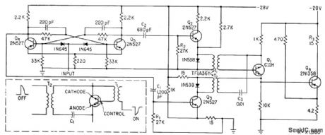
Power transistor 06 switches 20 W d-c through 15-ohm load R3 under control of scr Q1, which in turn is controlled by start-stop pulse amplifiers Q2 and Q3, and multivibrator Q4-Q5. Switching rote can be up to 700 cps.-J. E. Roberts, Controlled Recliners for Fost Power Switching, Electronics, 35:17, p 58-59. (View)
View full Circuit Diagram | Comments | Reading(632)
Inverting_comparator_with_hysteresis
Published:2009/7/24 4:20:00 Author:Jessie
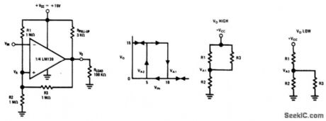
Fig. 15-5 This circuit provides positive feedback to force the comparator into a rapid state change when the input reaches the reference point. This overcomes one of the basic problems found in comparators (such as that in Fig. 15-1). Without feedback, the comparator can stay within the region between output high and low states (if the input is a slowly varying low-level signal). This might cause oscillation because a comparator is basically an uncompensated high-gain op amp. Only three resistors are required for feedback. The state changes are shown by the hysteresis graph. National Semiconductor Linear Applications Handbook 1991, p 258. (View)
View full Circuit Diagram | Comments | Reading(0)
Automatic_shutdown_for_abnormal_inputs110_V_220_V
Published:2009/7/24 4:20:00 Author:Jessie
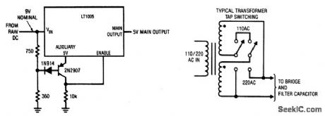
This circuit is useful in systems or instruments that can be powered from 110 V or 220 V (with a changeover switch). If a regulator is powered from 220 V with the switch set at 110 V, the regulator is forced to dissipate abnormal power, which causes thermal shutdown and possible damage. This circuit senses abnormally high input voltages and shuts down the regulator before thermal shutdown occurs. Normally, the input voltage is low enough to keep the transistor on, pulling the enable pin toward the auxiliary output and maintaining regulator output. If the circuit is inadvertently powered from 220 V, with the switch at 110V, VIN rises. This cuts off the transistor, and the 10-kΩ resistor pulls the enable pin to ground and shuts down the regulator. The diode prevents VBE from zenering during the reverse-bias condition, which exists during shutdown. For the values shown, the circuit functions over ranges of 88 to 135 Vac and 180 to 260 Vac (110 to 220 Vac ±20%). (View)
View full Circuit Diagram | Comments | Reading(743)
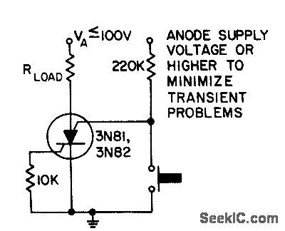
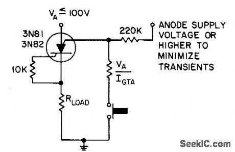
HYBRID_SWITCH_PROVIDES_1500_V_PULSE
Published:2009/7/24 4:19:00 Author:Jessie
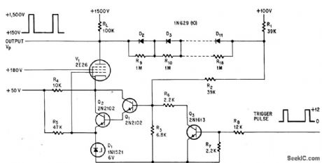
Trigger pulse at 12 V saturates Q3, voltage across R3 drops below level of tenor D1, and Q1 and Q2 turn off, making V1 stop conducting. Anode voltage of V1 then rises to 1,500-V supply value until input pulse is removed.-R. E. Thomas, 1,500-Volt Hybrid Switch has Low On Impedance, Electronics, 37:22, p 74-75. (View)
View full Circuit Diagram | Comments | Reading(650)
Precision_level_detector_for_photodiode
Published:2009/7/24 4:19:00 Author:Jessie
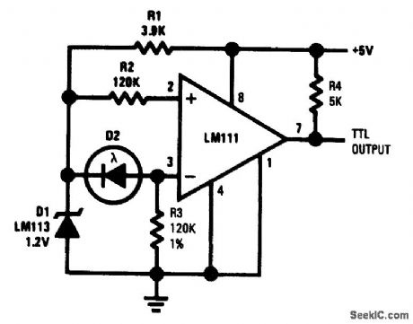
Fig. 15-4 This circuit is similar to that of Fig. 15-3, except that the Fig. 15-4 circuit is independent of supply voltage. D1 is a temperature- compensate d reference diode with a 1.23-V breakdown voltage. D1 acts as a regulator and delivers a stable voltage to the comparator. The circuit operates with a 5-V supply and is suitable for TTL. National Semiconductor, Linear Applications Handbook 1991 p, 130.
(View)
View full Circuit Diagram | Comments | Reading(857)
SCR_REED_A_C_SWITCH
Published:2009/7/24 4:18:00 Author:Jessie
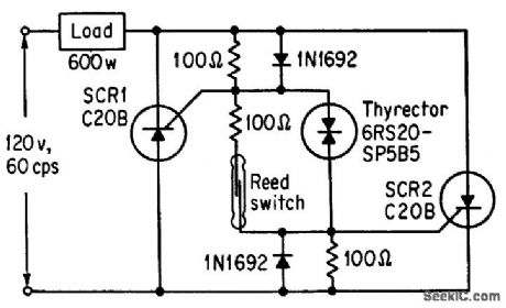
Magnetic reed switch makes ideal trigger for silicon controlled rectifiers, even though nine components are required for switching 600.w load.-M. P. Southworth, Bidirectional Static Switch Simplifies Ac Control, Control Engineering, March 1964, p 75-76. (View)
View full Circuit Diagram | Comments | Reading(790)
TRANSISTOR_SWITCHED_IGNITION
Published:2009/7/24 4:18:00 Author:Jessie
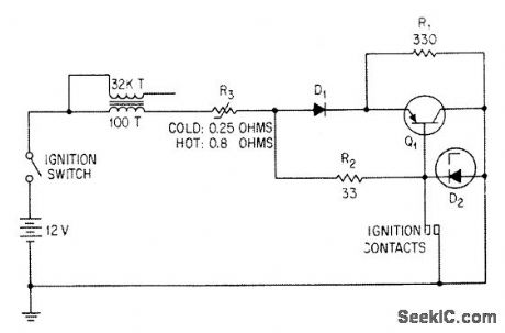
Ignition breaker points handle only current of about 0.25 amp for switching transistor Q1, in-creasing contact life, while transistor handles 9-amp peak ignition coil current. Diode D1 reverse-biases emitter-base junction when distributor contacts are open, to ensure transistor cutoff at high temperaturs. Zener D2 dips peaks of transients that might damage transistor.-S. B. Gray, Home and Auto Controls, Electronics, 36:19, p 52-56. (View)
View full Circuit Diagram | Comments | Reading(2515)
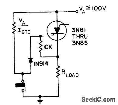
UNGROUNDED_SWITCH_SCS_CONTACT_ISOLATOR
Published:2009/7/24 4:26:00 Author:Jessie
Eliminates contact bounce when switch is dosed to trigger scs, because load current increases rapidly and latches on.- Transistor Manual, Seventh Edition, General Electric Co., 1964, p 433. (View)
View full Circuit Diagram | Comments | Reading(699)
A_C_POWER_INTERLOCK
Published:2009/7/24 4:26:00 Author:Jessie
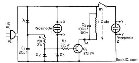
Any device drawing over 5 W (up to amount allowed by D2-D3) will produce 60-cps square wave at base of 01 when device is turned on, to energize relay through Q1 and apply power to receptacle 2.-C. J. Ulrick, AC Power Interlock, EEE, 13:6, p 65. (View)
View full Circuit Diagram | Comments | Reading(944)
Interfacing_a_comparator_to_ECL
Published:2009/7/24 4:26:00 Author:Jessie
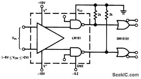
Fig. 15-12 This circuit shows how a high-speed comparator (LM161) that is designed for operation with TTL can be interfaced directly to ECL. National Semiconductor Linear Applications Handbook. 1991 p 326. (View)
View full Circuit Diagram | Comments | Reading(713)
Automatic_shutdown_during_power_outages
Published:2009/7/24 4:25:00 Author:Jessie
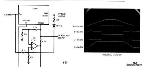
This circuit is useful when data bits must be transferred and stored into nonvolatile memory during power outages. The circuit takes advantage of the differing dropout voltages between the main and auxiliary outputs. When power is first applied, VIN (trace A in Fig. 9-6B) starts to rise (ramp up). The auxiliary output (trace D) follows this ramp action, and clamps at 5 V. During this interval, C1 monitors the difference between VIN and the 5-V auxiliary output. The resistor ratios are scaled so that the enable pin (trace B) is clamped until VIN is high enough to support main-output regulation. The small ramp segments that are visible at the enable pin are caused by the failure of C1 to clamp under a very low supply-voltage condition, and do not affect operation. The main output (trace C) comes up quickly. Because the auxiliary output precedes the main output, the auxiliary can be used to present conditions in the circuits being powered. When power falls below the threshold point, C1 pulls the enable pin low and forces the main output (trace C) off rapidly. However, the auxiliary output (trace D) maintains regulation after the main output is off. This allows the main output to be used as a logic signal to alert auxiliary-powered nonvolatile memory to store data. The amount of time that the auxiliary output will maintain regulation on power-down is controlled by the regulator tilter-capacitor size. The diode/4.7-kΩ combination provides regenerative action to ensure a clean turn-off for the main output. (View)
View full Circuit Diagram | Comments | Reading(740)
GROUNDED_SWITCH_SCS_CONTACT_ISOLATOR
Published:2009/7/24 4:25:00 Author:Jessie
Eliminates contact bounce when switch is closed to trigger scs, because load current increases rapidly and latches on.- Transistor Manual, Seventh Edition, General Electric Co., 1964, p 433. (View)
View full Circuit Diagram | Comments | Reading(690)
Comparator_for_signals_of_opposite_polarity
Published:2009/7/24 4:25:00 Author:Jessie
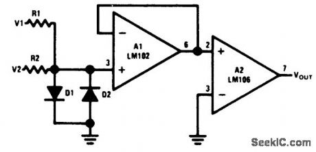
Fig. 15-11 In this circuit, R1 and R2 isolate the two signal sources. Often, such resistors must be relatively large so that the signal sources are not loaded (when fed directly to a comparator). As a result, the input current of the comparator must be reduced to prevent inaccuracies. The problem is eliminated with a buffer because the input current to the LM106 has no effect on the current through R1 and R2. National Semiconductor, Linear Applications Handbook. 1991, p. 1990. (View)
View full Circuit Diagram | Comments | Reading(651)
SCS_CONTACI_ISOLATOR_2
Published:2009/7/24 4:25:00 Author:Jessie
Eliminates contact t bounce when switch is closed to trigger scs, with both switch and load grounded.- Transistor Manual, Seventh Edition, General Electric Co., 1964, p 433. (View)
View full Circuit Diagram | Comments | Reading(599)
SCS_CONTACT_ISOLATOR_1
Published:2009/7/24 4:24:00 Author:Jessie
Eliminates contact bounce when both switch and load are grounded and opening of switch triggers scs. - Transistor Manual, Seventh Edition, General Electric Co., 1964, p 433. (View)
View full Circuit Diagram | Comments | Reading(657)
ac_coupled_comparator
Published:2009/7/24 4:24:00 Author:Jessie
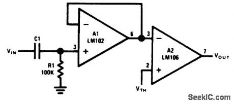
Fig. 15-10 This circuit also buffers the input of an LM106 with an L102 voltage follower. The LM106 draws an input current that is twice the specified bias current when the signal is above the comparison threshold. This asymmetrical current drain charges a coupling capacitor that is connected directly to the LM106 input and it can produce an error. The problem is eliminated with a buffer because the input current to the LM106 is both low and constant. National Semiconductor. Linear Applications Handbook 1991 p. 1190. (View)
View full Circuit Diagram | Comments | Reading(1077)
Zero_crossing_detector_with_low_input_current
Published:2009/7/24 4:23:00 Author:Jessie
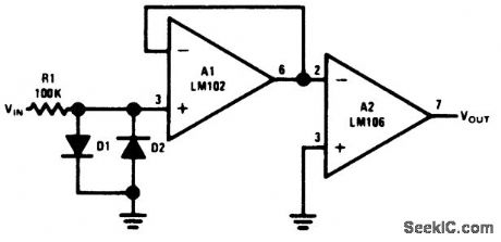
Fig. 15-9 This circuit buffers the input of an LM106 with an LM102 voltage follower. Such an arrangement reduces effective input current of the LM106 comparator by more than three orders of magnitude without greatly reducing speed. The high input currents of many comparators result in reduced speed when used with high source resistances. If the input signal can exceed the common-mode range of the comparator (±5 V for the LM106), clamp diodes must be used as shown. It is then necessary to isolate the comparator from the input with a relatively large resistance to prevent loading. National semiconductor Linear Applications Handbook,1991,p. 1190. (View)
View full Circuit Diagram | Comments | Reading(1120)
5_V_POWER_SUPPLY
Published:2009/7/24 4:23:00 Author:Jessie
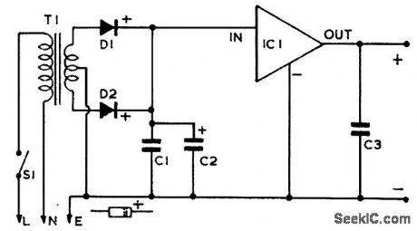
The 5-V power supply shown here will provide voltage-regulated power for digital ICs needing up to 500 mA. With the 5-V power supply constructed as a separate unit, any circuit to be operated can be plugged in, and this allows it to provide power for various projects. It can also be used where a 5-Vdc, 500-mA supply is suitable, so it can, in some cases, be pressed into service where a 4.5- or 6-V battery would otherwise be fitted. (View)
View full Circuit Diagram | Comments | Reading(672)
FAST_SWITCHING_OF_A_C_POWER
Published:2009/7/24 4:23:00 Author:Jessie
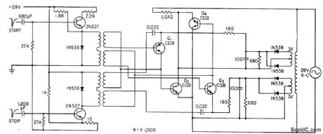
Pulsed scr's Q1 and Q2 turn on load-current-carrying scr's Q3 and Q4 under control of start-stop pulses from an external vibrator that feeds the 2N527 start-stop pulse amplifiers. Each pulsed scr has its own 3-V source. Load being switched requires 350 ma at 400 cps.-J. E. Roberts, Controlled Rectifiers for Fast Power Switching, Electronics, 35:17, p 58-59. (View)
View full Circuit Diagram | Comments | Reading(743)
| Pages:1191/2234 At 2011811182118311841185118611871188118911901191119211931194119511961197119811991200Under 20 |
Circuit Categories
power supply circuit
Amplifier Circuit
Basic Circuit
LED and Light Circuit
Sensor Circuit
Signal Processing
Electrical Equipment Circuit
Control Circuit
Remote Control Circuit
A/D-D/A Converter Circuit
Audio Circuit
Measuring and Test Circuit
Communication Circuit
Computer-Related Circuit
555 Circuit
Automotive Circuit
Repairing Circuit