
Circuit Diagram
Index 1187
MULTIPLE_ALARM_CIRCUIT
Published:2009/7/1 3:38:00 Author:May
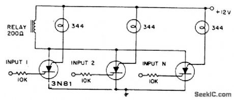
Any of several inputs pulls in the common alarm relay with lamps giving visual indication of triggering input. Low resistance lamps decrease input sensitivity. (View)
View full Circuit Diagram | Comments | Reading(977)
AUTO_BURGLAR_ALARM
Published:2009/7/1 3:37:00 Author:May
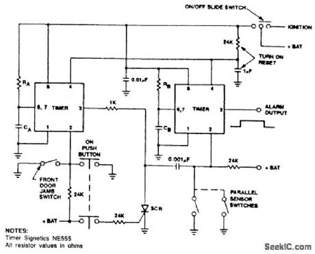
Timer A produces a safeguard delay, allowing the driver to disarm the alarm and eliminating a vulnerable outside control switch. The SCR prevents timer A from triggering timer B, unless timer B is triggered by strategically-located sensor switches. (View)
View full Circuit Diagram | Comments | Reading(0)
CRYSTAL_OSCILLATOR_PROVIDES_LOW_NOISE
Published:2009/7/1 3:35:00 Author:May
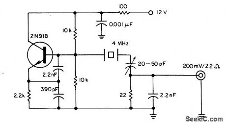
The oscillator delivers an output of high spectral purity without any substantial sacrifice of the usual stability of a crystal oscillator. The crystal in addition to determining the oscillator's frequency, is used also as a low-pass filter for the unwanted harmonics and as a bandpass filter for the sideband noise. The noise bandwidth is limited to less than 100 Hz. All higher harmonics are substantially suppressed-60 dB down for the third harmonic of the 4-MHz fundamental oscillator frequency. (View)
View full Circuit Diagram | Comments | Reading(874)
IC_COMPATIBLE_CRYSTAL_OSCILLATOR
Published:2009/7/1 3:33:00 Author:May
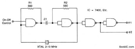
Resistors R1 and R2 temperature-stabilize the NAND gates; they also ensure that the gates are in a linear region for starting. Capacitor C1 is a dc block; it must have less than1/10 ohm impedance at the operating frequency. The crystal runs in a series-resonant mode. Its series resistance must be low; AT-cut crystals for the 1-to 10-MHz range work well. The output waveshape has nearly a 50% duty cycle, with chip-limited rise times. The circuit starts well from 0°to 70℃. (View)
View full Circuit Diagram | Comments | Reading(941)
SIMPLE_24_h_CLOCK
Published:2009/7/1 3:29:00 Author:May
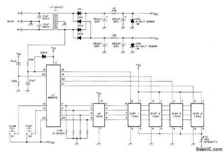
Use of 60-Hz power frequency as time base simplifies design while still giving Iong-term accuracy comparable to that of crystal time base. Four-digit display uses Hewlett-Packard 5082-7340 displays requiring only simple four-Iine BCD input. National MM5312N IC divides Iine frequency down to one pulse per minute and advances its internal storage register at same rate. Output of register is in binary form at pins 1, 2, 3, and 24, synchronized with digit-enable outputs at pins 18, 19, 20, and 21. Binary data is thus applied to all four displays in parallel, with enable lines controlling data feed. SN7404N inverter converts binary output data to TTL level required by displays.Power supply provides +5 V and -12 V for ICs and 60-Hz reference for clock check. CR5 is Radio Shack 276-561, CR6 is 276-563, and CR1-4 are 276-1146.-K. Powell, 24-Hour Clock with Digital Readout and Line-Frequency Time Base, Ham Radio, March 1977, p 44-48
(View)
View full Circuit Diagram | Comments | Reading(1696)
PRECISE_WAVE_GENERATOR
Published:2009/7/1 3:29:00 Author:May
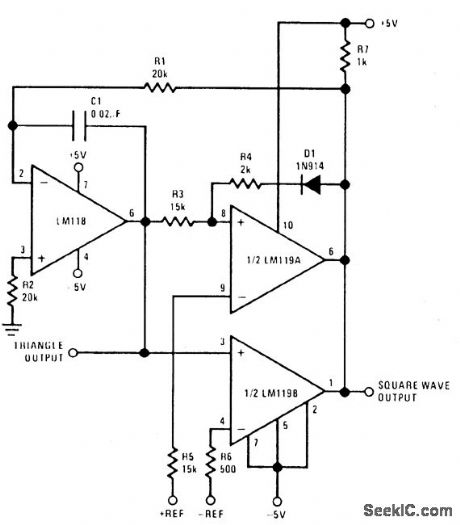
The positive and negative peak amplitude is controllable to an accuracy of about ±0.01 V by a dc input. Also, the output frequency and symmetry are easily adjustable. The oscillator consists of an integrator and two comparators-one comparator sets the positive peak and the other the negative peak of the triangle wave. If R1 is replaced by a potentiometer, the frequency can be varied over at least a 10 to 1 range without affecting amplitude. Symmetry is also adjustable by connecting a 50 kΩ resistor from the inverting input of the LM118 to the arm of the 1 kΩ potentiometer. The ends of the potentiometer are connected across the supplies. Current for the resistor either adds or subtracts from the current through R1,changing the ramp time. (View)
View full Circuit Diagram | Comments | Reading(719)
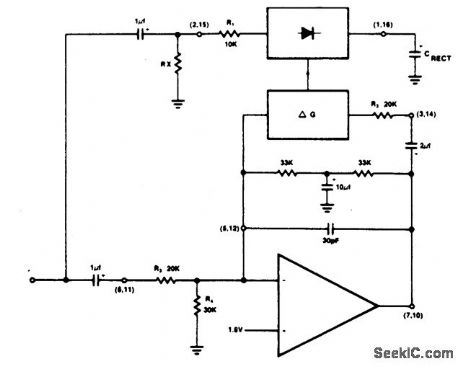
SIMPLE_FREQUENCY_TO_VOLTAGECONVERTER(10_kHz_FULL_SCALE,±0006_NON_LINEARITY)
Published:2009/7/1 3:28:00 Author:May
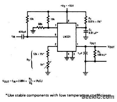
View full Circuit Diagram | Comments | Reading(849)
O_9_s_DIGITAL_READOUT
Published:2009/7/1 3:27:00 Author:May
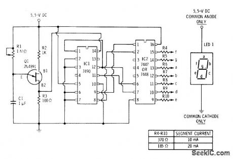
Can be used for classroom demonstration of digital logic driving 7-segment LED or as attention-getting desk display time base Q1 feeds sequential timing pulses to 7490 decade counter. Pulses are counted in binary mode, and bit pattern corre-sponding to digits 0-9 is fed to 7447 binary-to-decimal decoder/driver connected to 7-segment readout. Calibrate with watch or with timing reference signals from WWV, adjusting R1 so display advances 1 digit per second.-F. M.Mints, Electronic Circuitbook 5: LED Projects, Howard W. Sams, Indianapolis, IN, 1976, p 72-75. (View)
View full Circuit Diagram | Comments | Reading(5251)
ALARM_GENERATOR
Published:2009/7/1 3:26:00 Author:May
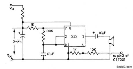
Simple 555 timer generates alarm tone driving small loudspeaker, for use with Cal-Tex CT7001 and other similar digital clocks which do not have internal tone generator. Circuit requires +5 V, but supply can be higher value if suitable dropping resistor is used.-M. S. Robbins, Electronic Clocks and Watches, Howard W. Sams, Indianapolis, IN, 1975,p 91. (View)
View full Circuit Diagram | Comments | Reading(945)
12_h_ALARM
Published:2009/7/1 3:24:00 Author:May
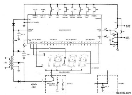
General-purpose digital clock with alarm uses National MM5402 or MM5405 MOS IC to drive 31/2-digit LED display and provide drive for alarm. Brightness control is optional. Sleep output can be used to turn off radio after desired time interval of up to 59 min.- MOS/LSI Databook, National Semiconductor,Santa Clara,CA,1977,p 1-68-1-73. (View)
View full Circuit Diagram | Comments | Reading(4757)
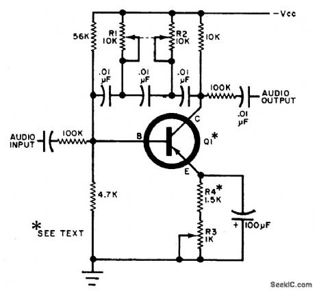
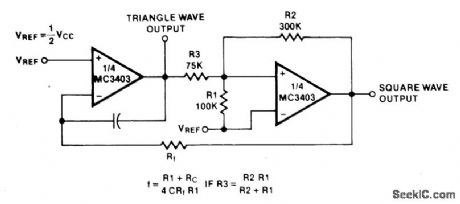
SINGLE_SUPPLY_FUNCTION_GENERATOR
Published:2009/7/1 3:23:00 Author:May
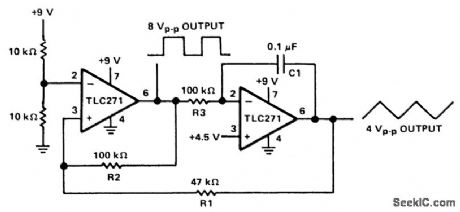


The circuit has both square-wave and triangle-wave output. The left section is similar in function to a comparator circuit that uses positive feedback for hysteresis. The inverting input is biased at one-half the VCC voltage by resistors R4 and R5. The output is fed back to the non-inverting input of the first stage to control the frequency. The amplitude of the square wave is the output swing of the first stage, which is 8 V peak-to-peak.The second stage is basically an op amp integrator. The resistor R3 is the input element and capacitor C1 is the feedback element. The ratio RI/R2 sets the amplitude of the triangle wave, as referenced to the square-wave output. For both waveforms, the frequency of oscillation can be determined by the equationThe output frequency is approximately 50 Hz with the given components. (View)
View full Circuit Diagram | Comments | Reading(1865)
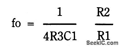
4_h_DIGITAL_WATCH
Published:2009/7/1 3:22:00 Author:May
Single Motorola MC14521 CMOS IC drives single-digit MAN 3 LED display in such a way that time range of 4 h is obtained wIth 1.875 min resolution. Can be built into old watch case at cost under $10 for parts.Oscillator frequency of 1.165 kHz can be tweaked to ad just dock, or crystal oscillator can be added for high accuracy. Analog/binary format of readout provides deciphering challenge to user, even though article gives diagram showing which segments of LED are lit for each time reading. Time intenrals represented by each lit segment of display are: B = 2 h; C = 1 h; A = 30 min; F = 15 min; G = 7.5 min; E = 3.75 min; D = 1.875 min.-R. M. Steimle, Small CMOS Digital Watch Has Analog LED Output, EDN Magazine, Aug. 20, 1976, p 86. (View)
View full Circuit Diagram | Comments | Reading(2806)
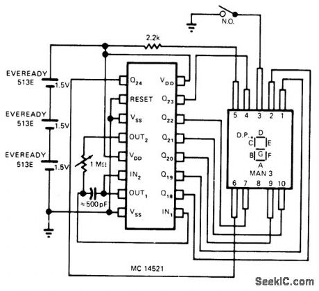
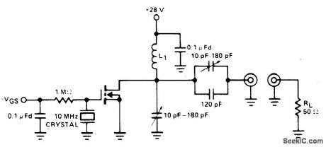
PIERCE_CRYSTAL_OSCILLATOR
Published:2009/7/1 3:22:00 Author:May


The JFET Pierce oscillator is stable and simple. It can be the clock of a microprocessor, a digital timepiece or a calculator. With a probe at the output, it can be used as a precise injection oscillator for troubleshooting. Attach a small length of wire at the output and this circuit becomes a micropower transmitter. (View)
View full Circuit Diagram | Comments | Reading(3212)
1_MHz_FET_CRYSTAL_OSCILLATOR
Published:2009/7/1 3:21:00 Author:May
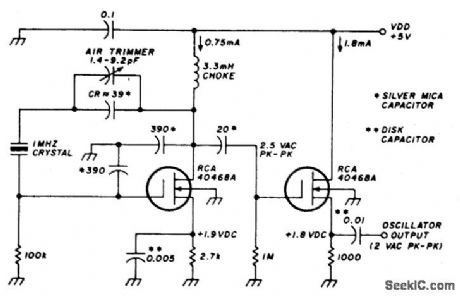
This stable oscillator circuit exhibits less than 1 Hz frequency change over a VDD range of 3-9 volts. Stability is attributed to the use of MOSFET devices and the use of stable capacitors. (View)
View full Circuit Diagram | Comments | Reading(2365)
CRYSTAL_CONTROLLED_SIGNAL_SOURCE
Published:2009/7/1 3:18:00 Author:May


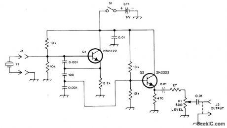
This general purpose signal source serves very well in signal-tracing applications.The output level is variable to more than 1 Vrms into a 50 Ω load. Almost any crystal in the 1 to 15 MHz range can be used. Q1 forms a Colpitts oscillator with the output taken from the emitter. A capacitive voltage divider (across the 2.2 K emitter resistor) reduces the voltage applied to the buffer amplifier, Q2. The buffer and emitter follower, provides the low input impedance necessary to drive 50 Ω loads.
(View)
View full Circuit Diagram | Comments | Reading(962)
CRYSTAL_OSCILLATOR
Published:2009/7/1 3:16:00 Author:May
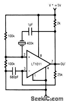
This circuit uses an LT1011 comparator biased in its linear mode and a crystal to establish its resonant frequency. This circuit can achieve a few hundred kHz, temperature independent clock frequency with nearly 50% duty cycle. (View)
View full Circuit Diagram | Comments | Reading(0)
FUNCTION_GENERATOR
Published:2009/7/1 3:16:00 Author:May
View full Circuit Diagram | Comments | Reading(0)
CRYSTAL_CONTROLLED_LOCAL_OSCILLATOR_FOR_SSB_TRANSMITTER
Published:2009/7/1 3:15:00 Author:May
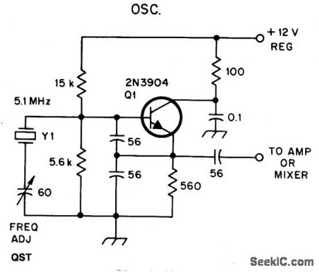


This oscillator may contain several switched crystals to provide channelized operation.A buffer amplifter may be added, if desired.
(View)
View full Circuit Diagram | Comments | Reading(925)
LOW_POWER,_5_V_DRIVEN,TEMPERATURE_COMPENSATED_CRYSTAL_OSCILLATOR(TXCO)
Published:2009/7/1 3:13:00 Author:May
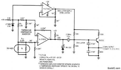
View full Circuit Diagram | Comments | Reading(844)
10_MHz_CRYSTAL_OSCILLATOR
Published:2009/7/1 3:11:00 Author:May


This xtal oscillator is a FET equivalent of a vacuum tube tuned to plate-tuned grid xtaloscillator. Feedback is via the drain to gate capacitance. (View)
View full Circuit Diagram | Comments | Reading(1071)
| Pages:1187/2234 At 2011811182118311841185118611871188118911901191119211931194119511961197119811991200Under 20 |
Circuit Categories
power supply circuit
Amplifier Circuit
Basic Circuit
LED and Light Circuit
Sensor Circuit
Signal Processing
Electrical Equipment Circuit
Control Circuit
Remote Control Circuit
A/D-D/A Converter Circuit
Audio Circuit
Measuring and Test Circuit
Communication Circuit
Computer-Related Circuit
555 Circuit
Automotive Circuit
Repairing Circuit