
Circuit Diagram
Index 1199
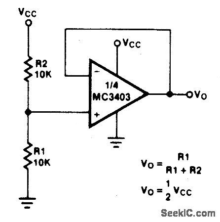
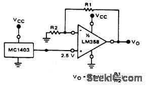
VOLTAGE_REFERENCE_1
Published:2009/7/1 2:08:00 Author:May
View full Circuit Diagram | Comments | Reading(619)
NiCad_charger_for_grounded_batteries
Published:2009/7/24 5:12:00 Author:Jessie
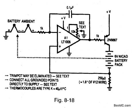
Figure 8-18 showp a thermally based NiCad charger for use with batteries that are common to ground. The transistor is connected as a common emitter, so the inputs to A1 are reversed. However, operation is the same as for the Fig. 8-15 circuit. Notice that in both the Fig. 8-15 and 8-18 circuits, the trimpot can be eliminated by specifying an LT1006 set (at manufacture) to the desired offset value. High-quality grounds must be used, and all ground returns must be brought directly back to the supply common terminal. LINEAR TECHNOLOGY, APPLICATION NOTE 37, PAGE 2.
(View)
View full Circuit Diagram | Comments | Reading(788)
BIPOLAR_DC_DC_CONVERTER_REQUIRES_NO_INDUCTOR
Published:2009/7/1 2:08:00 Author:May
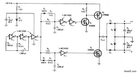


Inverters Ula and Ulb form a 20-kilohertz oscillator whose square wave output-further shaped by D2, R4, and R5 and by D3, R6, and R7-drives power field-effect transistors Q2 and Q3. The p-channel and n-channel FETs conduct alternately, in a push-pull configuration. When Q2 conducts, the positive charge on Cout forces diode D4 to conduct as well, which produces a positive voltage, determined by zener diode D5, at terminal A. Similarly, when Q3, in its turn conducts, the negative charge on Cout forces D7 to do so as well. A negative voltage, therefore, develops at terminal B, whose level is set by D6. (View)
View full Circuit Diagram | Comments | Reading(1186)
High_precision_weight_scale
Published:2009/7/24 5:11:00 Author:Jessie
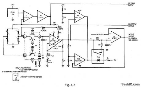
Figure 4-7 shows a switched-capacitor type of bridge circuit used in weight-scale applications. (The circuit is intended for weighing human subjects.) Resolution is 0.01 pound at 300.00 pounds, full scale. To trim the circuit, adjust the zero pot for 0 V out with no weight on the platform. Then set the gain adjustment for 3.0000-V output for a 300.00-pound platform weight. Repeat this procedure until both points are fixed. LINEAR TECHNOLOGY, APPUCAT;ON NOTE 43, P. 8. (View)
View full Circuit Diagram | Comments | Reading(1945)
VOLTAGE_REFERENCE
Published:2009/7/1 2:08:00 Author:May
View full Circuit Diagram | Comments | Reading(1369)
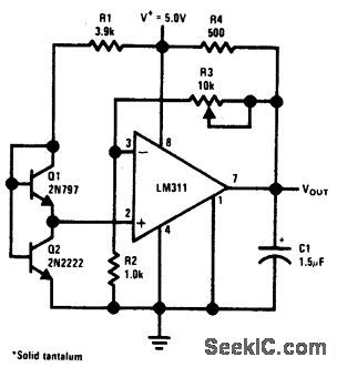
Thermally_based_NiCad_charger
Published:2009/7/24 5:10:00 Author:Jessie

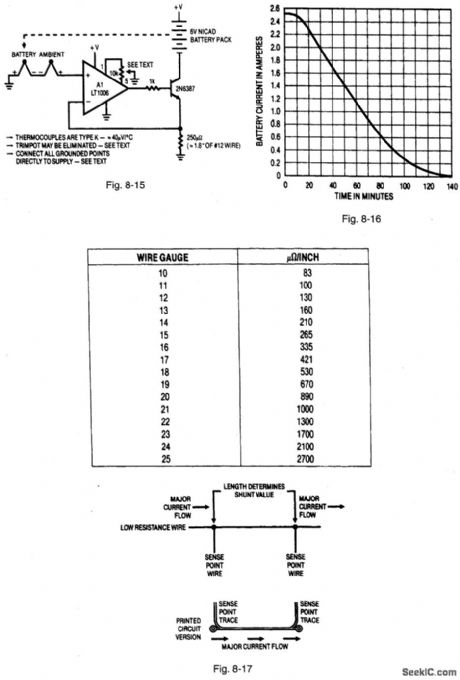
Figure 8-15 shows a simple thermally based charging circuit for NiCad batteries.Figure 8-16 shows the charge characteristics.Thermocouples sense both cell andambient temperature simultaneously. A1 provides the amplification necessary for microvolt-level thermocouple signals. The 10-kΩ trimpot is set to introduceenough input-off set so that the A1 output swmgs positive turning on thetransistor. Figure 8-17 shows a simple, lnexpenslve way to construct low-resistance shunts usmg a small length of wlre or a PC trace.The type and length of wire determines the shunt resistance (which can be altered to produce the desiredcharging characteristics). Figure 8-17 also shows resistance-versus-len gth characteristics for varlous wire sizes, as well as the details for both wlre and PC shunts.In both cases (PC or wire) the shunt should have separate connections for sensing (Kelvin style) SO that high current does not affect the readings.LINEARTECHNOLOGY, APPLICATION NOTE 37.P.4. (View)
View full Circuit Diagram | Comments | Reading(666)
MULTIPLEXED_CLOCK_DlSPLAY
Published:2009/7/1 2:08:00 Author:May
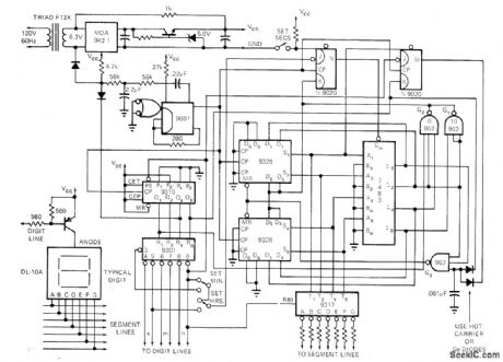
Multiplexed display suitable for LED readouts is provided by circuit using TTL counters to count 60-Hz Iine.When count reaches 10 o'clock, flip-flop M is set on evely cycle. Gate G3 then detects when time goes to 13 o'clock, and clears shift register.Carry flip-flop remains set, so 1 is loaded into hours digit to accomplish transition from 12:59:59 to 1:00:00. Seven-segment decoder driver Iooks at shift register output and drives segment lines of LED Leading hours digit is blanked,using RBI input on 9317.-G.Smith,Novel clock Circuit Provides Multiplexed Display,EDN Magazine.Sept 1,1972,p 50-51.
(View)
View full Circuit Diagram | Comments | Reading(2664)
IC_battery_backup_rechargeable_battery
Published:2009/7/24 5:10:00 Author:Jessie
This circuit is similar to that of Fig.9-19,except that a trickle charge is applied to a rechargeable battery(through the diode and resistor). (View)
View full Circuit Diagram | Comments | Reading(951)
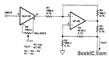
NONINVERTING_BIPOLAR_CURRENT_SOURCE
Published:2009/7/1 2:07:00 Author:May
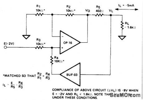
View full Circuit Diagram | Comments | Reading(781)
High_resolution_single_supply_bridge_amplifier
Published:2009/7/24 5:10:00 Author:Jessie
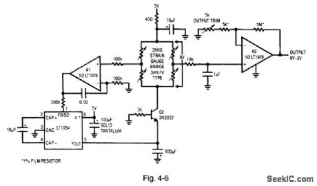
Figure 4-6 shows a high-resolution version of the Fig, 4-5 circuit. The Fig. 4-6 circuit uses a bipolar positive-to-negative converter, which has much lower output impedance. The biasing used permits 8 V to appear across the bridge, requiring the 100-mA capability of the LT1054 to sink about 24 mA. This increased drive results in a more favorable transducer-gain per slope, increasing the signal-to-noise ratio. LINEAR TECHNOLOGY, APPLICATION NOTE 43, P. 7. (View)
View full Circuit Diagram | Comments | Reading(765)
LOW_VOLTAGE_ADJUSTABLE_REFERENCE_SUPPLY
Published:2009/7/1 2:07:00 Author:May
View full Circuit Diagram | Comments | Reading(664)
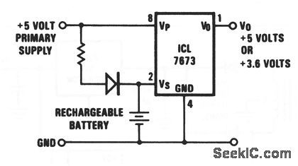
IC_battery_backup_lithium_battery
Published:2009/7/24 5:09:00 Author:Jessie
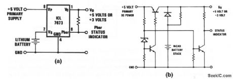
The circuit of Fig.9-19A uses single ICL7873 to replace a typical discrete-component battery-backup system, such as shown in Fig. 9-19B. (View)
View full Circuit Diagram | Comments | Reading(1716)
BILATERAL_CURRENT_SOURCE_1
Published:2009/7/1 2:05:00 Author:May
View full Circuit Diagram | Comments | Reading(641)
Single_supply_bridge_amplifier_with_common_mode_suppression
Published:2009/7/24 5:09:00 Author:Jessie
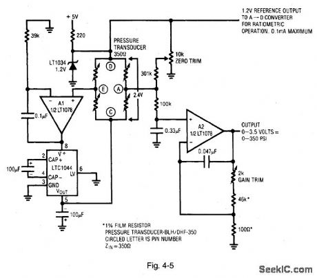
Figure 4-5 shows a circuit that is similar to that of Fig. 4-4, except that a single power supply is required. A2 biases the LTC1044 positive-to-negative converter. The LTC1044 output pulls the bridge output negative, causing the Al input to balance at 0 V. This local loop permits a single-ended amplifier (A2) to extract the bridge output signal. The 100-k℃/033-μF RC filter minimizes noise. The A2 gain is set to provide the desired output scale factor. Because bridge drive is taken from the LT1034 reference, the A2 output is not affected by supply shifts. The LT1034 output is available for ratio operation. Although the supply is 5 V, the transducer sees only 2.4 V of drive. This reduced drive results in lower transducer outputs for a given measurement value, effectively magnifying amplifier offset-drift terms. The limit on the available bridge drive is set by the CMOS LTC1044 output impedance. LINEAR TECHNOLOGY, APPLICATION NOTE 43, P. 7. (View)
View full Circuit Diagram | Comments | Reading(760)
LINEAR_VARIABLE_DIFFERENTIAL_TRANSFORMER_SIGNAL_CONDITIONER
Published:2009/7/1 2:05:00 Author:May
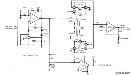
A1 and its associated components furnish an amplitude stable she wave source. A1's positive feedback path is a Wein bridge, tuned for 1.5 kHz, Q1, the LT1004 reference, and additional components in Al's negative loop unity-gain stabilize the amplifier. A1's output an amplitude stable sine wave, drives the LVDT. C1 detects zero crossings and feeds the LTC1043 clock pin. A speed-up network at C1's input compensates LVDT phase shift, synchronizing the LTC1043's clock to the transformer's output zero crossings. The LTC1043 alternately connects each end of the transformer to ground, resulting in positive half-wave rectification at pins 7 and 14. These points are summed at a low-pass filter which feeds A2. A2 furnishes gain scaling and the circuit's output.The LTC1043's synchronized clocking means the information presented to the low-pass filter is amplitude and phase sensitive. The circuit output indicates how far the core is from center and on which side. To calibrate this circuit, center the LVDT core in the transformer and adjust the phase trim for 0 V output. Next, move the core to either extreme position and set the gain trim for 2.50 V output. (View)
View full Circuit Diagram | Comments | Reading(1814)
PRECISION_VOLTAGE_TO_FREQUENCY_CONVERTER
Published:2009/7/1 2:05:00 Author:May

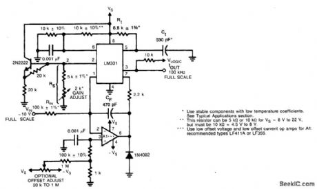
In this circuit, integration is performed by using a conventional operational amplifier and feedback capacitor, CF. When the integrator's output crosses the nominal thresh-old level at pin 6 of the LM131, the timing cycle is initiated. The average current fed into the op amp's summing point (pin 2) is i × (1.1 RtCt) × fwhich is perfectly balanced with -VIN/RIN. In this circuit, the voltage offset of the LM131 input comparator does not affect the offset or accuracy of the V-to-F converter as it does in the stand-alone V-to-F converter, nor does the LM131 bias current or offset current. Instead, the offset voltage and offset current of the operational amplifier are the only limits on how small the signal can be accurately converted.
(View)
View full Circuit Diagram | Comments | Reading(1068)
CIRCULAR_LED_ARRAY
Published:2009/7/1 2:04:00 Author:May
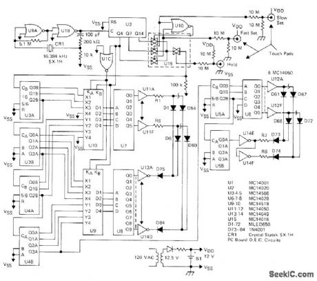
Arrangement of 60 LEDs sequencing in outer ring to indicate seconds and minutes, combined with 12 in inner ring to indicate hours, is driven by Motorola MC14566 CMOS industrial time-base generator.Time reference is 16.384-kHz crystal oscillator consisting of two NOR gates and Statek crystal.Reference frequency is divided by 214 in U2 to give 1-s pulse rate for driving accumulators U3A-U5B. Maximum error is 1 s per month. U3 counts seconds, U4 minutes, and U5 hours.Multiplexing is required because same set of 60 LEDs serves for minutes and seconds. Fast and slow touch pads eliminate need for switches when setting time. Single 12-V nicad battery provides backup for AC line failure.-A. Mou-ton, The LED Circular Timepiece, Motorola, Phoenix, AZ, 1975. EB-41. (View)
View full Circuit Diagram | Comments | Reading(1962)
QUAD_op_AMP_GENERATES_FOUR_DIFFERENT_SYNCHRONIZED_WAVEFORMS_SIMULTANEOUSLY
Published:2009/7/1 2:03:00 Author:May
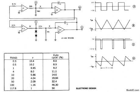
A quad op amp can simultaneously generate four synchronized waveforms. The two comparators (A1 and A3) produce square and pulse waves, while the two integrators (A2 and A4) give triangular and sawtooth waves. Resistor R1 sets the duty cycle and the frequency, along with resistors R and capacitors C. (View)
View full Circuit Diagram | Comments | Reading(1347)
PROGRAMMABLE_VOLTAGE_SOURCE_1
Published:2009/7/1 2:02:00 Author:May
View full Circuit Diagram | Comments | Reading(606)
INEXPENSIVE_FREQUENCY_COUNTER_TACHO_METER
Published:2009/7/1 2:02:00 Author:May
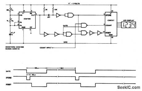
Circuit NotesThis circuit uses the low power ICM7555(CMOS 555)to generate the gating,STORE and RESET signals,To provide the gating stgnal,the timer IS configured as an astable multivibrator. The system is calibrated by using a 5 M potentiometer for Ra as a coarse control and a 1 jk potentiometer for Re as a fine control.CD40106B's are used as a monostable multivibrator and reset time delay. (View)
View full Circuit Diagram | Comments | Reading(797)
| Pages:1199/2234 At 2011811182118311841185118611871188118911901191119211931194119511961197119811991200Under 20 |
Circuit Categories
power supply circuit
Amplifier Circuit
Basic Circuit
LED and Light Circuit
Sensor Circuit
Signal Processing
Electrical Equipment Circuit
Control Circuit
Remote Control Circuit
A/D-D/A Converter Circuit
Audio Circuit
Measuring and Test Circuit
Communication Circuit
Computer-Related Circuit
555 Circuit
Automotive Circuit
Repairing Circuit