
Circuit Diagram
Index 1198
Light_controlled_one_shot_timer
Published:2009/7/24 4:57:00 Author:Jessie
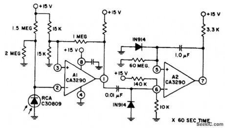
Fig. 15-38 In this circuit, comparator A1 is used to sense a change in photodiode current, and A2 operates as a one-shot timer and is triggered by A1. The A2 output switches low for about 60 seconds after the light source is interrupted. The circuit operates at normal room-lighting levels. Circuit sensitivity can be adjusted by changing the values of the l-MΩ/2-MΩ resistors, but the ratio of these resistors should be constant. Figures 15-30B and 15-30C show the pin connections and electrical characteristics, respectively. Harris Semiconductor Linear & Telecom ICs. 1991. p. 4-22. (View)
View full Circuit Diagram | Comments | Reading(695)
GROUND_TESTER
Published:2009/7/1 2:18:00 Author:May
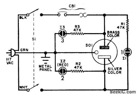
The circuit is simple and foolproof if wired correctly. Under normal conditions, only lamps 1 and 3 should be lit. If lamp 2 comes on, the cold lead is 117 volts above ground. (View)
View full Circuit Diagram | Comments | Reading(0)
Multiple_supply_fault_monitor
Published:2009/7/24 4:57:00 Author:Jessie
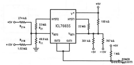
This circuit shows an overvoltage/undervoltage fault monitor for multiple supplies, using a single ICL7665S detector. Figure 9-15B shows the pin connections. The resistors are chosen such that the sum of the currents through R21A, R21B and R31 is equal to the current through R11 when the two input voltages are at the desired low-voltage detection point. The current through R11 at this point is equal to 1.3 V/R11. The voltage at the VSET input depends on the voltage of both supplies being monitored. The trip voltage of one supply (while the other supply is at the nominal voltage) will be different than the trip voltages when both supplies are below their normal voltages. The other side of the ICL7665S can be used to detect the absence of negative supplies. The trip points for OUT1 depend on both the negative supply voltages and the actual voltage of the +5-V supply. (View)
View full Circuit Diagram | Comments | Reading(832)
DIGITAL_ALARM
Published:2009/7/1 2:16:00 Author:May

Direct drive offered by Fairchild 3817 IC allows design of simple Iow-cost clock radio providing display drive, alarm, and sleep-to-music features in 12- or 24-h formats.Display is Fairchild FND500 LED. Either 50- or 60-Hz input may be used. U2 is 7800-series IC volt-age regulator rated to meet requirements of radio used. Q3 provides active low output for timed radio turnoff after user-selected interval of up to 59 min. CR4 and C5 rectify alarm-tone output for amplification by Q4 to give active low output for timed radio turn-on when coincidence is detected by alarm comparators. Q5 provides alarm-tone output at level sufficient to drive 40-ohm loudspeaker with ample wake-up volume. If radio is used, omit loudspeaker. Article covers construction and adjustment.-D.Ft. Schmieskors, Jr., Low-Cost Digital Clock, Ham Radio, Feb. 1976,p 26-30.
(View)
View full Circuit Diagram | Comments | Reading(6472)
Comparator_Schmitt_trigger
Published:2009/7/24 4:56:00 Author:Jessie
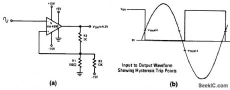
Fig. 15-37 This circuit is essentially a zero-crossing detector with hysteresis. The circuit has a 100-mV hysteresis, which can be used in applications, where very fast transition times are required at the output-even though the input signal is very slow. The hysteresis loop also reduces false triggering because of noise on the input. The waveforms in Fig. 15-37B show the trip points developed by the hysteresis loop. Figures 15-32B and 15-32C show the pin connections, and electrical characteristics, respectively. Harris semiconductor, Linear & Telecom ICs. 1991. p. 4-30. (View)
View full Circuit Diagram | Comments | Reading(1958)
MEASURING_PHASE_DIFFERENCE_FROM_0°to±180°
Published:2009/7/1 2:15:00 Author:May
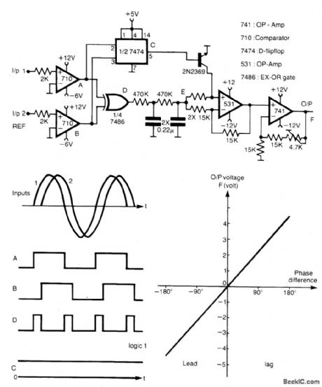
This method is capable of measuring phase between 0 to ±180°. The generated square waves A and B are fed to a D flip-flop which gives an output C equal to logic 1 when input 1 leads input 2 and equal to logic 0 in case of lagging. When C = logic 0, the output of the amplifier F will be positive proportional to the average value E of the output of the EX-OR. When C = logic 1, F will be negative and also proportional to E by the same factor. Hence, the output of the meter is positive in case of lagging and negative for leading. The circuit is tested for sinusoidal inputs and indicates a linearity within l%. Measurements are unaffected by the frequency of the inputs up to 75 kHz. (View)
View full Circuit Diagram | Comments | Reading(1094)
AC_DC_CLOCK
Published:2009/7/1 2:14:00 Author:May

When AC power fails, MCD-2 optoisolator senses voltage drop and makes Schmitt trigger force strobe input of clock chip to ground, blanking display and reducing current P' ain from 2O0 mA on AC to 12 mA on 9-V standby battery. Clock will run for days on 1000-mAh battery. Two LED pairs that form colons between time dighs are operated from digit strobe Iines and remain lit when display is blanked, but draw only 1 mA.-S. l. Green, Dig-ital Clock Keeps Counting Even When AC Power Fails, EDN Magazine, Dec, 20, 1974, p 49-51. (View)
View full Circuit Diagram | Comments | Reading(1422)
DIODE_TESTING
Published:2009/7/1 2:14:00 Author:May
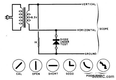
The circuit will display curves on a scope, contingent on the state of the diode. To calibrate, substitute a 1000-ohm resistor for the diode and adjust the scope gains for a 45-degree line. The drawings show some expected results. (View)
View full Circuit Diagram | Comments | Reading(870)
WIRE_TRACER
Published:2009/7/1 2:14:00 Author:May
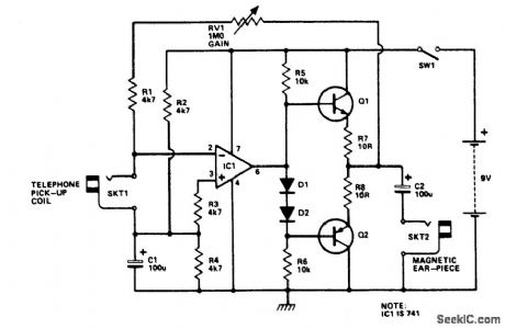
The tracer detects the weak magnetic field of any current-carrying house wiring and amplifies this signal to a level that is adequate for driving a magnetic earpiece. The unit uses a telephone pick-up coil to detect the magnetic field. (View)
View full Circuit Diagram | Comments | Reading(4484)
LINEAR_TRIANGLE_SQUARE_WAVE_VCO
Published:2009/7/1 2:13:00 Author:May
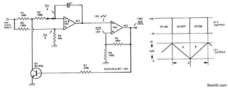
The VCO has two buffered outputs; a triangle wave and a square wave. Frequency is dependent on the output voltage swing of the Schmitt trigger, IC2. Superior performance can be obtained by replacing Q1 with a switching FET. Fast FET op amps will improve high frequency performance. (View)
View full Circuit Diagram | Comments | Reading(4019)
LOW_POWER_REGULATOR_REFERENCE
Published:2009/7/1 2:11:00 Author:May
This simple reference circuit provides a stable voltage reference almost totally free of supply voltage hash. Typical power supply rejection exceeds 100 dB. (View)
View full Circuit Diagram | Comments | Reading(1163)
RESISTANCE_RATIO_DETECTOR
Published:2009/7/1 2:11:00 Author:May
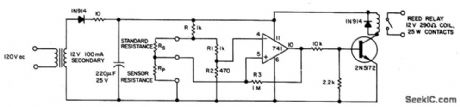
Applications such as photoelectric control, temperature detection and moisture sensing require a circuit that can accurately detect a given resistance ratio. A simple technique that uses an op amp as a sensini element can provide 0.5% accuracy with low parts cost. The reed-relay contacts close when the resistance of the sensor Rp equals 47% of the standard Rs. Adjusting either R1 or R2 provides a variable threshold; the threshold is controlled by varying R3. For the most part, the type of resistors used for R1 and R2 determines the accuracy and stability of the circuit. With metal-ftlm resistors, less than 0.5% change in ratio sensing occurs over the commercial temperature range (0 to 70 C) with ac input variations from 105 to 135 V. (View)
View full Circuit Diagram | Comments | Reading(1123)
Nonvolatile_low_voltage_indicator
Published:2009/7/24 5:15:00 Author:Jessie
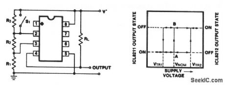
In this circuit, the high-trip voltage VTR2 is set above the normal supply-voltage range. On power-up, the initial condition is A. When S1 is closed momentarily, the operating point changes to B, and remains at B until the supply voltage drops below VTR1, at which time the output reverts to A. Notice that state A is always retained if the supply voltage is reduced below VTR1 (even to 0 V) and then raised back to VNOM. Figure 9-21B shows the equations to calculate resistor values. (View)
View full Circuit Diagram | Comments | Reading(651)
STANDBY_SUPPLY
Published:2009/7/1 2:10:00 Author:May
Phase-shift oscillator Ql operates from AC line through bridge-rectifier power supply and provides line-synchronized 60-Hz power to standard digital clock through isolating emitter-follower Q2. Curing power outage, oscillator is switched automatically to battery by diode network and provides reason-ably accurate signal for operating clock. Free-running oscillator is adjusted to be slightly Iow, such as 59.9 Hz. For reasonably Iong power outage, say 4 h, this 0.1-Hz error is equivalent to 0.167% error in time, so clock loses only 24 s during outage. C1 and C2 are 200 to 300 μF. Ad-just R1 to give output just below 60 Hz on battery operation. To minimize battery drain, LEDs on digital clock are not energized during standby.-R. S. Isenson, Digital Clock Fail-Safe, 73 Magazine, July 1977, p 168-169. (View)
View full Circuit Diagram | Comments | Reading(807)
Linearized_platinum_RTD_resistance_bridge
Published:2009/7/24 5:14:00 Author:Jessie
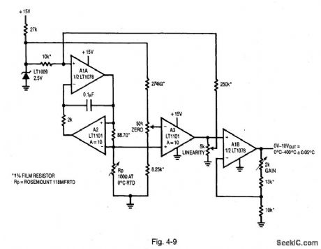
Figure 4-9 shows a bridge with a ground-referred RTD to Improve noise rejection,The RTD leg is driven by a current Source, with the opposite bridge branch voltage biased.The current drive allows the bridge voltage across the RTD to vary directly with the temperature-induced resistance shift. The difference between this potential and that of the opposing bridge leg forms the bridge output,To calibrate, substitute a precision decade box(General Radio 1432k)for RP. Set the box to the0℃ value(100.00Ω)and adjust the offset trim for a 0.00-V output. Then set the decade box for a 140℃ output(154.26Ω)and adjust the gain trim for a 3.500-V output reading, Finally, set the box to 249.0V-Ω(400.00℃)and trim the linearity adjustment for a 10.000-V output. Repeat the sequence until all three points are fixed.The total error over the entire range will be within ±0.05℃. The resistance values given are for a nominal 100.00 Ω(0℃)sensor. Sensors deviating from this nominal value can be used by factoring In the deviation from 100.00Ω.LINEARTECHNOLOGY,APPLICATION NOTE 43,P. 11. (View)
View full Circuit Diagram | Comments | Reading(807)
OSCILLATOR_OR_AMPLIFIER_WITH_WIDE_FREQUENCY_RANGE
Published:2009/7/1 2:09:00 Author:May
An oscillator/amplifter is resistively tunable over a wide frequency range. Feedback circuits containing operational amplifiers, resistors, and capacitors synthesize the electrical effects of an inductance and capacitance in parallel between the input terminals. The synthetic inductance and capacitance, and, therefore, the resonant frequency of the input admittance, are adjusted by changing a potentiometer setting. The input signal is introduced in parallel to the noninverting input terminals of operational amplifiers A1 and A2 and to the potentiometer cursor. The voltages produced by the feedback circuits in response to input voltage V1 are indicated at the various circuit nodes. (View)
View full Circuit Diagram | Comments | Reading(742)
Switch_mode_thermally_based_NiCad_charger
Published:2009/7/24 5:13:00 Author:Jessie
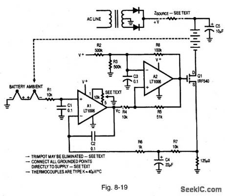
Figure 8-19 shows a thermally based NiCad charger operated in the switching mode. The circuits of Figs. 8-15 and 8-18 both force the transistor to dissipate some power, and the resulting heat might be a problem in a small enclosure (typical of micropower circuits). The circuit of Fig. 8-19 relies on the source impedance of the wall transformer to limit current through Q1 and the battery pack. The source impedance can be set when specifying the transformer. LINEAR TECHNQLOGY, APPLICATION NOTE 37, P. 3. (View)
View full Circuit Diagram | Comments | Reading(904)
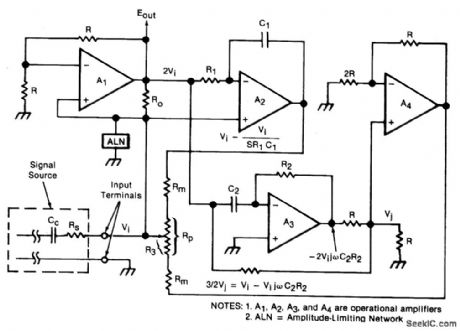
Floating_input_bridge
Published:2009/7/24 5:12:00 Author:Jessie

Figure 4-8 shows an optically coupled switched-capacitor bridge with a floating input. The common-mode rejection ratio at dc for the front-end exceeds 160 dB. The amplifier operates over a ±200-V common-mode range. Gain-accuracy and stability are limited only by external resistors. The offset drift is 0.05-μV/℃. The optical drive to the MOSFET eliminates the charge-injection problems that are common to FET switched-capacitor networks. LINEAR TECHNOLOGY, APPLICATION NOTE 43, P, 10. (View)
View full Circuit Diagram | Comments | Reading(878)
MAGNETOMETER
Published:2009/7/1 2:08:00 Author:May
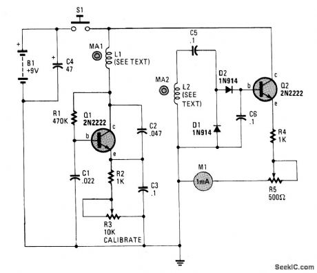
The circuit uses two general-purpose npn transistors, Q1 and Q2, and a special hand-wound, dual-coil probe ferrets out the magnetism. Q1 and its associated components form a simple VLF oscillator circuit, with L1, C2, and C3 setting the frequency. The VLF signal received by the pickup coil, L2, is passed through C5 and rectified by diodes Dl and D2. The small dc signal output from the rectifier is fed to the base of Q2 (conftgured as an emitter follower), which is then fed to a 0-1 mA meter, M1. (View)
View full Circuit Diagram | Comments | Reading(6408)
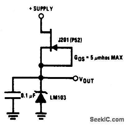
Low_voltage_battery_indicator_
Published:2009/7/24 5:12:00 Author:Jessie
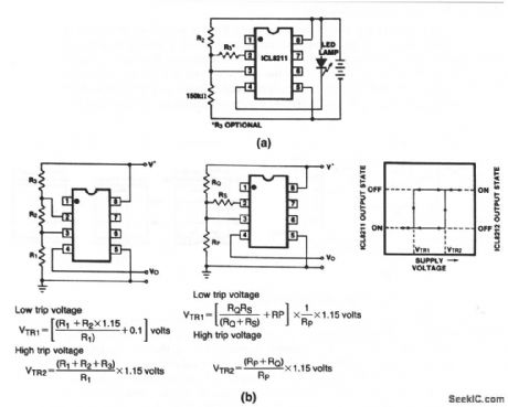
This application is particularly suitable for portable or remotely operated equipment, which requires an indication of a depleted or discharged battery. The quiescent current is typically 35 μA, which increases to 7 mA when the LED is turned on. R3 is optional and provides hysteresis if desired. Figure 9-21B shows the equations to calculate resistor values. (View)
View full Circuit Diagram | Comments | Reading(967)
| Pages:1198/2234 At 2011811182118311841185118611871188118911901191119211931194119511961197119811991200Under 20 |
Circuit Categories
power supply circuit
Amplifier Circuit
Basic Circuit
LED and Light Circuit
Sensor Circuit
Signal Processing
Electrical Equipment Circuit
Control Circuit
Remote Control Circuit
A/D-D/A Converter Circuit
Audio Circuit
Measuring and Test Circuit
Communication Circuit
Computer-Related Circuit
555 Circuit
Automotive Circuit
Repairing Circuit