
Circuit Diagram
Index 1184
DATE_DETECTOR
Published:2009/7/1 4:08:00 Author:May
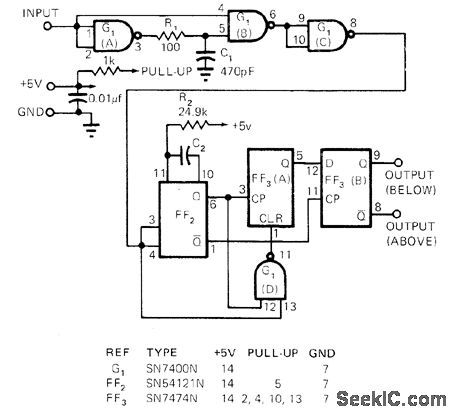
Only three ICs are used to sense pulse rate of input signal with high accuracy,For monitoring frequency, two such circuits can be used, with one set to upper frequency limit and other to lower limit. Output is high when input pulse rate is above set point and low for frequencies below set point. Frequency of set point is reciprocal qf monostable delay time (f0 = 1/0.32R2 C2).-J. W. Poore,Three IC′s Accurately Sense Pulse Rate,EDN Magazine, Aug. 15, 1972, p 53. (View)
View full Circuit Diagram | Comments | Reading(908)
POWER_GaAsFET_AMPLIFIER_WITH_SINGLE_SUPPLY
Published:2009/7/1 4:08:00 Author:May
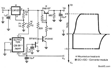
The dual regtilator circuit operates from a positive supply, which when switched ON powers the gate first, and when switched OFF shuts off the drain first as shown in the figure. This circuit incorporates the LM123, a three terminal positive regulator and a dc + to dc - converter, the outputs of which power the drains and gates of the power GaAsFETs in a power amplifier relay. The output of the three terminal regulator drives a dc + to dc - converter whose output biases an N-channel JFET suitably so as to pull the base of the series pass transistor 2N6107 to a level to turn it on. The circuit will turn off the drain supply whenever the negative potential on the Gate fails. (View)
View full Circuit Diagram | Comments | Reading(795)
CURRENT_SENSING_IN_suPPLY_RAILS
Published:2009/7/1 4:06:00 Author:May
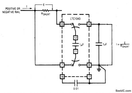
The LTC1043 can sense current through a shunt in either of its supply rails. This capability has wide application in battery and solar-powered systems. If the ground-referred voltage output is unloaded by an amplifier, the shunt can operate with very little voltage drop across it, minimizing losses. (View)
View full Circuit Diagram | Comments | Reading(675)
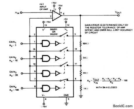
PRECISION_WEIGHTED_RESISTOR_PROGRAMMABLE_GAIN_AMPLIFIER
Published:2009/7/1 4:05:00 Author:May
View full Circuit Diagram | Comments | Reading(926)
STEREO_AMPLIFIER_WITH_GAIN_CONTROL
Published:2009/7/1 4:05:00 Author:May
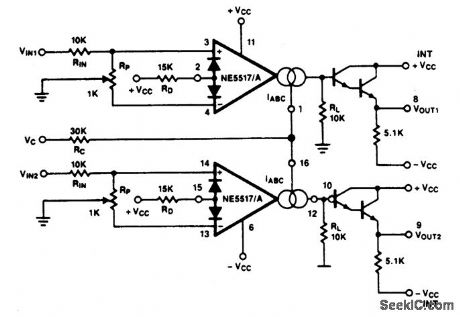
Excellent tracking of typical 0.3 dB is easy to achieve. With the potentiometer, RP, the offset can be adjusted. For ac-coupled amplifiers, the potentiometer may be replacGd with two 5.1 k ohm resistors. (View)
View full Circuit Diagram | Comments | Reading(691)
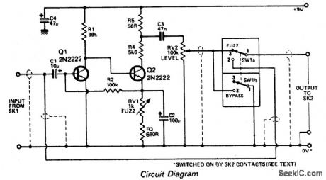
GUITAR_FUZZ
Published:2009/7/1 4:04:00 Author:May
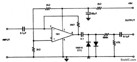
Circuit Notes
The 741 has a maximum gain of 20,000,but the circuit is so designed that the IC’s gain is 2,700,000 which then distorts the output. This distortion gnres the fuzz effect. The two diodes clip the output to drop the level, also lowered by the potential divider. This circuit also sustains the notes, due to clipping, giving a totally new sound. (View)
View full Circuit Diagram | Comments | Reading(988)
SWITCHING_CAPACITANCE_TRANSDUCERS
Published:2009/7/24 4:00:00 Author:Jessie
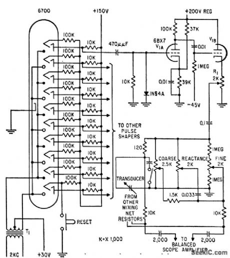
Beam-switching tube pulses bridges sequentially. Each bridge has pressure-sensitive capacitance transducer that unbalances bridge in proportion to changes in pressure. Outputs of bridges are displayed as pulse pattern corresponding to pattern of pressure imposed on auto seat.-A. Stiebel, High-Speed Switching of Low level Signals, Electronics, 32:12, p 54-55.
(View)
View full Circuit Diagram | Comments | Reading(633)
1_μS_PULSE
Published:2009/7/1 4:03:00 Author:May
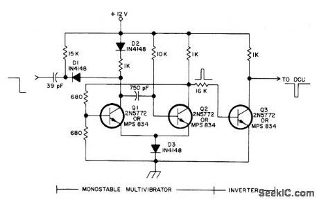
Monostable MVBR converts negative-going event signal into pulses having standardized width of about 1 μs, inverted by 03 for use as input to counter.-T. E. Hutchin-son. Inexpensive Decimal Counting Unit, 73 Magazine. Jan. 1974. p 47-51. (View)
View full Circuit Diagram | Comments | Reading(596)
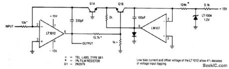
COMPOSITE_AMPLIFIER
Published:2009/7/1 4:03:00 Author:May
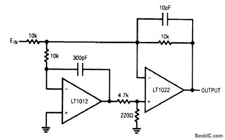
The circuit is made up of an LT1012 low drift device, and an LT1022 high speed amplifter. The overall circuit is a unity gain inverter, with the summing node located at the junction of three 10 k resistors. The LT1012 monitors this summing node, compares it to ground, and drives the LT1022's positive input, completing a dc stabilizing loop around the LT1022. The 10 k - 300 pF time constant at the LT1012 limits its response to low frequency signals. The LT1022 handles high frequency inputs while the LT1012 stabilizes the dc operating point. The 4.7 k - 220 ohm divider at the LT1022 prevents excessive input overdrive during start-up. This circuit combines the LT1012's 35 μV offset and 1.5 V/℃ drift with the LT1022's 23 V/μs slew rate and 300 kHz full power bandwidth. Bias current, dominated by the LT1012, is about 100 pA. (View)
View full Circuit Diagram | Comments | Reading(1509)
Magnetic_pickup_signal_conditioner
Published:2009/7/24 4:00:00 Author:Jessie

Fig. 14-16 This circuit uses an LM2907 as a very simple signal conditioner for a magnetic pickup. This basic configuration provides a low-impedance output voltage that is proportional to input frequency. The linearity of this voltage is typically better than 0.3% of full scale. No calibration is required. National Semiconductor Linear Applications Handbook, 1991.p. 423. (View)
View full Circuit Diagram | Comments | Reading(2483)
AMMETER_WITH_SlX_DECADE_RANGE
Published:2009/7/1 4:03:00 Author:May
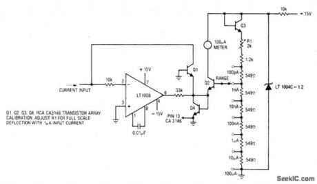
The Ammeter measures currents from 100 pA to 100 μA without the use of expensive high value resistors. Accuracy at 100 μA is limited by the offset voltage between Q1 and Q2 and, at 100 pA, by the inverting bias current of the LT1008 (View)
View full Circuit Diagram | Comments | Reading(1109)
OFF_LINE_REGULATOR
Published:2009/7/24 3:59:00 Author:Jessie
This circuit produces 8 to 12 Vdc using an off-line regulator. The ratio of the resistors determines the output voltage. The best value for R1 plus R2 is 250 kΩ, although the data sheet allows values between 200 and 300 kΩ. The 250-kΩ value minimizes loading, permitting the circuit to provide more accurate output voltage.WARNING: There is no isolation between line and load, and a potentially dangerous shock hazard exists. Do not use this circuit if the potential for accidental contact exists with the circuit and any other person or device. (View)
View full Circuit Diagram | Comments | Reading(844)
FUZZ_BOX_5
Published:2009/7/1 4:03:00 Author:May
Circuit Notes
Transistors Q1 and Q2 amplify the in- coming signal, and the gain is such that the input will overload when used with an electric guitar. RV1 adjusts the amount of feedback present, and hence voltage gain. The output is, therefore, a squared version of the input signal.The amount of squaring is varied by RV1. (View)
View full Circuit Diagram | Comments | Reading(818)
Acoustic_thermometer
Published:2009/7/24 3:59:00 Author:Jessie
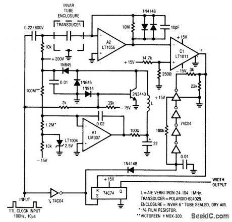


Fig. 14-15 Acoustic thermometry is used where extremes in operating temperature are encountered, such as in cryogenics and nuclear reactors. The transducer is composed of Polaroid ultrasonic material, mounted at one end of a sealed, 6-in long Invar tube. The medium inside the tube is dry air. The transducer can be considered a capacitor, composed of an insulating disc with conductive coating on each side. Each clock pulse causes mechanical movement of the disc, and ultrasonic energy is emitted. The clock pulse simultaneously resets the 74C74 output flip-flop. The ultrasonic energy travels down the tube, bounces off the far end, and returns to the transducer, causing mechanical displacement of the transducer. This shifts the transducer capacitance, resetting the 74C74 through A2 and C1. The 74C74 output pulse represents the transit time down the tube and it varies with the temperature, according to the equation:
C=331, √5T/273 meters/second, where C=speed of sound.
The pulse width (time between set and reset) can be converted into desired temperature information with a monitoring processor. Linear Technology. Linear Applications Handbook 1990. p AN7-5, (View)
View full Circuit Diagram | Comments | Reading(0)
LOGARITHMIC_AMPLIFIER_2
Published:2009/7/1 4:01:00 Author:May
View full Circuit Diagram | Comments | Reading(598)
CALENDAR_CLOCK
Published:2009/7/1 4:01:00 Author:May
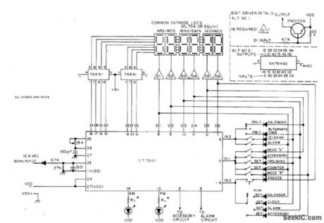
Uses Fairchild FCM7001 IC eauivalent of Cal-Tex CT7001 doek chip (which is no Ionger available) to drive six 7-segment LEDs that can be switched to show 12- or 24-h time and 28/30/31 calendar, along with alarm features. Article gives constluction details.Each SN75491 driver chip has pins 3, 5, 10, and 12 connected to pin 11 through 150-ohm resistor RL is typically 2,7K,chosen to limit LED current to less than 5 mA,-W,J. prudhomme,CT7001 Clockbuster,73 magazine,Dec,1976,p 52-54 and 56-58. (View)
View full Circuit Diagram | Comments | Reading(4521)
HIGH_SPEED_TRANSISTOR_RELAY
Published:2009/7/24 3:58:00 Author:Jessie
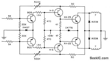
Push-pull switch handles up to 10 amp with rise time of 50 microsec. Rising d-c voltage at input produces no output until predetermined level is reached, when power supply voltage is suddenly switched across load. Circuit remains locked in until input voltage drops below trip level. Trip voltage is determined largely by breakdown voltage of 1N437 zener diode.-D. L. Anderson, Fast Transistor Relay, Electronics, 31:11, p 145. (View)
View full Circuit Diagram | Comments | Reading(798)
ULTRA_HIGH_ZSUBin_SUBAC_UNITY_GAIN_AMPLIFIER_
Published:2009/7/1 4:00:00 Author:May
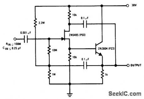
Nothing is left to chance in reducing inputcapacitance.The 2N5485,which has low capacitance in the first place,is operated db a sourcefollower with bootstrapped gate bias resistorand drain. (View)
View full Circuit Diagram | Comments | Reading(802)
12_OR_24_h_CLOCK
Published:2009/7/1 3:59:00 Author:May
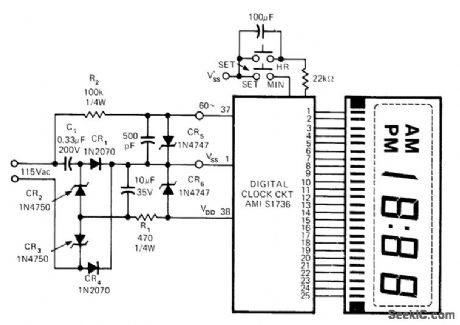
Single American Microsystems AMI S1736 clock chip drives Iiquidcrystal readout to give either 12-h display with AMjPM indicator or 24-h digital display by changing only three connections.-LSI in Con-sumer Applications, Round 2: Clocks on a Chip, EDN Magazine, May5, 1973, p22-23. (View)
View full Circuit Diagram | Comments | Reading(775)
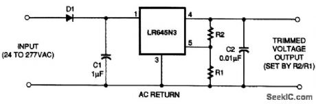
5_V_OFF_LINE_REGULATOR
Published:2009/7/24 3:58:00 Author:Jessie
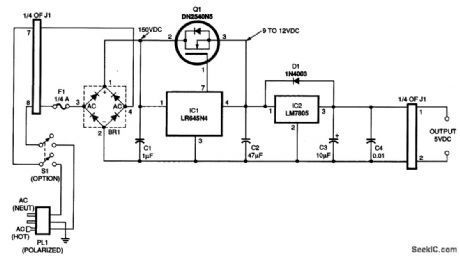
This circuit produces 5 Vdc using an off-line regulator. An input from 12 to 120 Vac is applied to pins 7 and 8 of the eight-pin circuit-board-mounted header (J1). Although the LR645N4 (IC1) accepts voltages up to 450 V, the input of this circuit is limited by the 200 PIV (peak inverse voltage) rating of the bridge rectifier (BR1). The full-wave-rectified input is applied to the 1-μF filter capacitor (C1). The filtered 150 Vdc is applied directly to pin 1 of IC1. Filter capacitance is unusually low because IC1 has a ripple rejection ratio (Vin/Vout) of 60 dB at 120 Hz with no load. The filtered input dc is also applied to pin 2 of the N-channel, depletion-mode MOSFET Q1, made by Supertex. It was designed to be compatible with LR6 linear regulators. MOSFET Q1 conducts up to 100 mA from the high-voltage source through the gate control line of the IC1, thus bypassing it. The combined regulated voltage and current source from Q1 and IC1 is then filtered through capacitor C2 to stabilize the regulated output. The regulated output of IC1 is applied to the LM340 (7805) voltage regulator (IC2) that regulates the output voltage of the combination of IC1 and Q1 to a logic-compatible 5 Vdc. The total available current at the 5-Vdc output is 100 mA, more than adequate current for most logic circuitry. The 5-Vdc is also filtered by 10-μF tantalum capacitor C3 for additional circuit stability under full current load.WARNING: There is no isolation between line and load, and a potentially dangerous shock hazard exists. Do not use this circuit if the potential for accidental contact exists with the circuit and any other person or device. (View)
View full Circuit Diagram | Comments | Reading(1603)
| Pages:1184/2234 At 2011811182118311841185118611871188118911901191119211931194119511961197119811991200Under 20 |
Circuit Categories
power supply circuit
Amplifier Circuit
Basic Circuit
LED and Light Circuit
Sensor Circuit
Signal Processing
Electrical Equipment Circuit
Control Circuit
Remote Control Circuit
A/D-D/A Converter Circuit
Audio Circuit
Measuring and Test Circuit
Communication Circuit
Computer-Related Circuit
555 Circuit
Automotive Circuit
Repairing Circuit