
Circuit Diagram
Index 1188
VARACTOR_TUNED_10_MHz_CERAMIC_RESONATOR_OSCILLATOR
Published:2009/7/1 3:09:00 Author:May
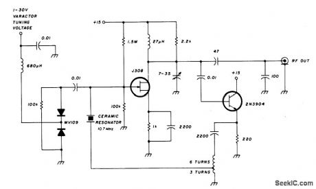
The FET input amplifier has fixed bias with source feedback. This provides a very high input impedance with very low capacitance. The FET amplifier drives an emitter follower which, in spite of the fact that it has a low output impedance, feeds a transformer with a 3:1 turns ratio for a nine-fold impedance reduction. The result is an impedance at the ceramic resonator of a few ohms maximum. The varactor-tuned ceramic resonator oscillator has a significant frequency-temperature coefficient. The tuning range of the VCO is approximately 232 kHz, with a temperature coefficient of 350 Hz per degree centigrade. When using this circuit as a VCO, the entire 232 kHz range cannot be used because some of the tuning range must be sacrificed for the temperature dependence.If the required tuning range were 200 kHz, leaving 32 kHz for temperature variation, the resulting temperature variation would be more than 90℃. (View)
View full Circuit Diagram | Comments | Reading(1951)
10_MHz_UNIVERSAL_COUNTER
Published:2009/7/1 3:07:00 Author:May
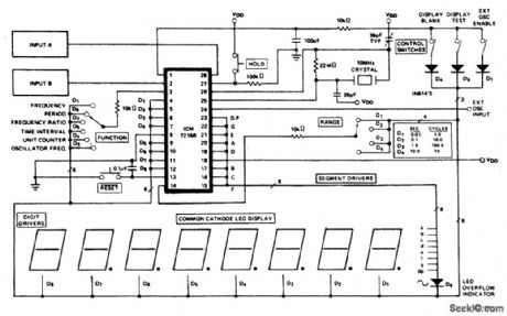
The ICM7216A or B can be used as a minimum component complete Universal Counter.This circuit can use input frequencies up to 10 MHz at INPUT A and 2 MHz at INPUTB If the signal at INPUT A has a very Iow duty cycle it may be necessary to use a 74121 monostable multivibrator or similar circuit to stretch the input pulse width to be able to guarantee that it is at least 50 ns in duration. (View)
View full Circuit Diagram | Comments | Reading(0)
LINEAR_RAMP_GENERATOR
Published:2009/7/1 3:04:00 Author:May
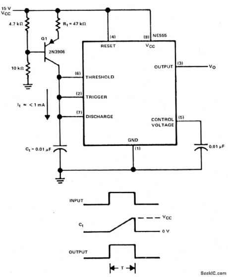
The linear charging ramp is most useful where linear control of voltage is required.Some possible applications are a long period voltage controlled timer, a voltage to pulse width converter, or a linear pulse width modulator. Q1 is the current source transistor, supplying constant current to the timing capacitor Ct. When the timer is triggered, the clamp on Ct is removed and Ct charges linearly toward VCC by virtue of the constant current supplied by Q1. The threshold at pin 6 is 2/3 VCC; here, it is termed VC. When the voltage across Ct reaches VC volts, the timing cycle ends. The timing expression for output pulse with T is:In general, It should be 1 mA value compatible with the NE555. (View)
View full Circuit Diagram | Comments | Reading(3256)
ATTENDANCE_COUNTER
Published:2009/7/1 3:03:00 Author:May
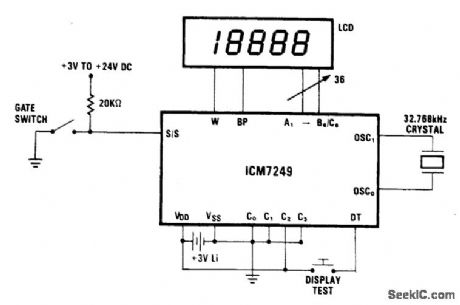
The display shows each increment. By using mode 2, external debouncing of the gate switch is unnecessary, provided the switch bounce is less than 35ms. The 3 V lithium battery can be replaced without disturbing operation if a suitable capacitor is connected in parallel with it. The display should be disconnected, if possible, during the procedure to minimize current drain. The capacitor should be large enough to store charge for the amount of time needed to physically replace the battery (t = VC/1). A 100 μF capacitor initially charged to 3 V will supply a current of 1.0 μA for 50 seconds before its voltage drops to 2.5 V, which is the minimum operating voltage for the ICM7249.Before the battery is removed, the capacitor should be placed in parallel, across the VDD and GND terminals. After the battery is replaced, the capacitor can be removed and the display reconnected. (View)
View full Circuit Diagram | Comments | Reading(0)
ANALOG_COUNTER_CIRCUIT
Published:2009/7/1 3:01:00 Author:May
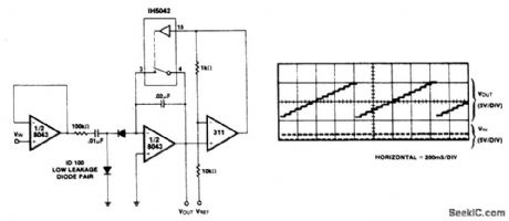
A straightforward circuit using a LM311 for the level detector and a CMOS analog gate to discharge the capacitor is shown. An important property of this type of counter is the ease with which the count can be changed; it is only necessary to change the volt-age at which the comparator trips. A low cost A-D converter can also be designed using the same principle since the digital count between reset periods is directly proportional to the analog voltage used as a reference for the comparator. A considerable amount of hysteresis is used in the comparator. This ensures that the capacitor is completely discharged during the reset period. In a more sophisticated circuit, a dual comparator window detector could be used, the lower trip point is set close to ground to ensure complete discharge. The upper trip point could then be adjusted independently to determine the pulse count.
(View)
View full Circuit Diagram | Comments | Reading(1411)
100_MHz_FREQUENCY,PERIOD_COUNTER
Published:2009/7/1 2:59:00 Author:May
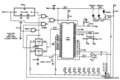
The figure shows the use of a CD4016 analog multiplex to multiplex the digital outputs back to the FUNCTION input. Since the CD4016 is a digitally controlled analog transmission gate, no level shifting of the digit output is required. The CD4051's or CD4052's could also be used to select the proper inputs for the multiplexed input on the ICM7226 from 2 or 3 bit digital inputs. These analog multiplexers may also be used in systems in which the mode of operation is controlled by a microprocessor rather than directly from front panel switches. TTL multiplexors such as the 74LS153 or 74LS251 may also be used, but some additional circuitry will be required to convert the digit output to TTL compatible logic levels. (View)
View full Circuit Diagram | Comments | Reading(4623)
WAVEFORM_GENERATOR
Published:2009/7/1 2:55:00 Author:May
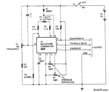
The circuit is designed around the Intersil 8038CC. Frequency range is approximately 20 Hz to 20 kHz-a tuning range of 1000:1 with a single control. The output frequency depends on the value of C2 and on the setting of potentiometer R1. Other values of C2 change the frequency range. Increase the value of C2 to lower the frequency. The lowest possible frequency is around.001 Hz and the highest is around 300 kHz. (View)
View full Circuit Diagram | Comments | Reading(1253)
BINARY_COUNTER
Published:2009/7/1 2:55:00 Author:May
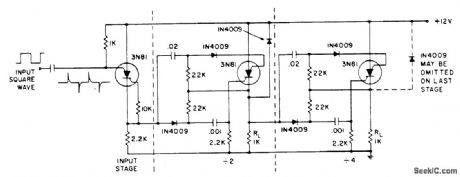
Stages are triggered by the positive going edge. The scs is tumed on at the cathode gate; turned off at the anode gate. The anode-to-cathode IN4009 suppresses positive transients while the scs is recovering. The input stage generates fast positive edges to trigger the counter. (View)
View full Circuit Diagram | Comments | Reading(0)
20_kHz_RING_COUNTER
Published:2009/7/1 2:53:00 Author:May
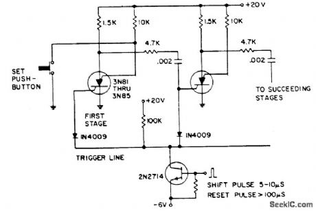
The shift pulse turns off the conducting scs by reverse biasing the cathode gate.The charge stored on the coupling capacitor then triggers the next stage. An excessively long shift pulse charges up all the capacitors, turning off all stages. Grounding an anode gate will set that stage. (View)
View full Circuit Diagram | Comments | Reading(656)
4_DIGIT_O7_INCH_LED_DlSPLAY
Published:2009/7/1 2:51:00 Author:May
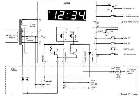
National MA1013 clock module contains MOS LSI clock IC, display, power supply, and associated discrete components on single printed-circuit board that is easily connected to radio. Operates from either 50-Hz or 60-Hz inputs, and gives either 12- or 24-h display format. Nonmulti-plexed LED drive eliminates RF interference.Display is flashed at 1-Hz rate after powerfailure of any duration, to indicate need for resetting dock. Zero appearing in first digit is blanked. On 12-h version, dot in upper left corner is ener-gized to indicate PM.- MOSiLSl Databook, National Semiconductor, Santa Clara, CA, 1977, p 13-23-13-28.
(View)
View full Circuit Diagram | Comments | Reading(700)
ASTABLE_MULTIVIBRATOR
Published:2009/7/1 2:51:00 Author:May
View full Circuit Diagram | Comments | Reading(0)
RING_COUNTER_WITH_VARIABLE_TIMING
Published:2009/7/1 2:50:00 Author:May
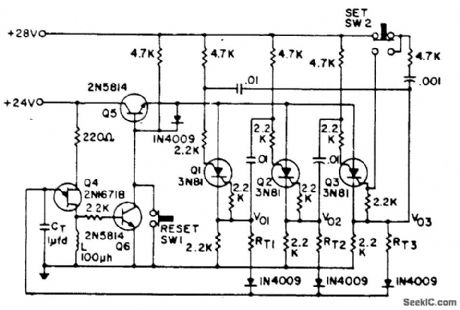


Shift pulses are generated by the unijunction transistors. The intervals between pulses are controlled by CT and RT. A different RTcan be selected for each stage of the counter as shown.
(View)
View full Circuit Diagram | Comments | Reading(1055)
BATTERY_BACKUP
Published:2009/7/1 2:49:00 Author:May
During normal operation, all power for dighal clock is provided by AC power supply. During power failure, clock con tinues operating from battery backup using two 9-V batteries in series. Battery drain is limited by diode CR2 that blocks power flow to displays. Optional switch may be installed across diode to short it for momentary viewing of display.-W. J. Prudhomme, CTT001 Clockbuster, 73 Magazine, Dec. 1976, p 52-54 and 56-58. (View)
View full Circuit Diagram | Comments | Reading(1071)
UJT_MONOSTABLE_CIRCUIT_INSESITIVE_TO_CHANGE_IN_BIAS_VOLTAGE
Published:2009/7/1 2:49:00 Author:May
View full Circuit Diagram | Comments | Reading(560)
DIGITAL_WRISTWATCH
Published:2009/7/1 2:48:00 Author:May
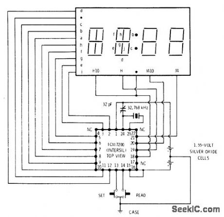
Single Intersil ICM7200 IC drives multiplexed display giving choice of hours and minutes, seconds, and day/date. CMOS chip divides 32.768-kHz crystal out-put in long internal binary divider to produce basic 1-s clock rate. Furtherdivision gives other elements of display. Pressing read button once gives hours and minutes;pressing second time gives day and date; and pressing third time gives seconds.-D. Lancaster, CMOS Cook-book, Howard W. Sams, Indianapolis, IN, 1977, p 377-378. (View)
View full Circuit Diagram | Comments | Reading(2271)
MONOSTABLE_USING_VIDEO_AMPLIFIER_AND_COMPARATOR
Published:2009/7/1 2:47:00 Author:May
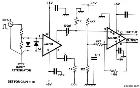
The output of a video amplifier is differentiated before being fed to a Schottky comparator. The propagation delay is reduced to typically 10ns. The output pulse width is set by the value of C, 100pf giving a pulse of about 90ns duration. (View)
View full Circuit Diagram | Comments | Reading(875)
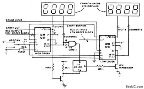
8_DIGIT_UP_DOWN_COUNTER
Published:2009/7/1 2:46:00 Author:May

This circuit shows how to cascade counters and retain correct leading zero blanking.The NAND gate etects whether a digit is active since one of the two segments a or bis active on any unblanked number. The flip flop is clocked by the least significant digit of the high order counter, and if this digit is not blanked, the Q output of the flip flop goes high and turns on the npn transistor, thereby inhibiting leading zero blanking on the low order counter. (View)
View full Circuit Diagram | Comments | Reading(1525)
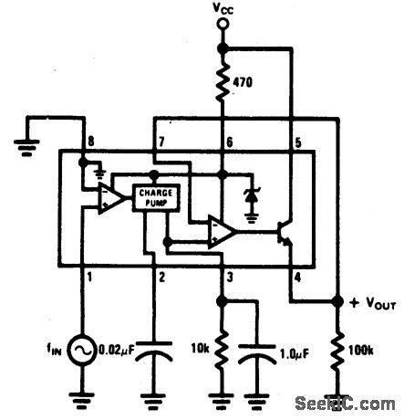
ZENER_REGULATED_FREQUENCY_TO_VOLTAGE_CONVERTER
Published:2009/7/1 2:44:00 Author:May
View full Circuit Diagram | Comments | Reading(560)
FREQUENCY_TO_VOLTAGE_CONVERTER(DIGITAL_FREQUENCY_METER)
Published:2009/7/1 2:43:00 Author:May

Circuit NotesThis circuit converts frequency to voltage by taking the average dc value of the pulses from the 74121 monostable multivibrator. The one shot is triggered by the positive-going ac signal at the input of the 529 comparator.The amplifier acts as a dc filter, and also provides zeroing. The accuracy is 2% over a 5 decade range. The input signal to the comparator should be greater than0.1 volt peak-to-peak, and less than12 volts peak-to-peak for proper operation. (View)
View full Circuit Diagram | Comments | Reading(3456)
AC_DIGITAL_CLOCK_WITH_STANDBY_BATTERY
Published:2009/7/1 2:43:00 Author:May
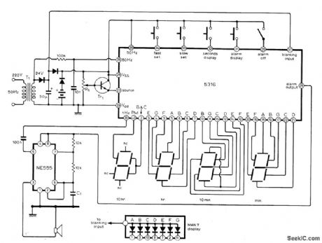
Uses MM5316 alarm-clock IC,originally designed to drive LCD or fluorescent displays,but modified here for LED display Diodes and batteries provide power if AC fails,with blanking of display to extend battery life. Accuracy is poor on batteries but batteries make resetting of time and alarm easier after AC interruption.Alarm uses 555 multivibrator to produce frequency-shfft warble on output tone. Time is set by fast and slow buttons, and alarm is set with same buttons while depressing alarm-display button. Transistor type is not critical.-M. F.Smith, Digital Alarm Clock, Wireless World, Nov. 1976, p 62.
(View)
View full Circuit Diagram | Comments | Reading(2620)
| Pages:1188/2234 At 2011811182118311841185118611871188118911901191119211931194119511961197119811991200Under 20 |
Circuit Categories
power supply circuit
Amplifier Circuit
Basic Circuit
LED and Light Circuit
Sensor Circuit
Signal Processing
Electrical Equipment Circuit
Control Circuit
Remote Control Circuit
A/D-D/A Converter Circuit
Audio Circuit
Measuring and Test Circuit
Communication Circuit
Computer-Related Circuit
555 Circuit
Automotive Circuit
Repairing Circuit