
Circuit Diagram
Index 1185
ULTRA_LOW_LEAKAGE_PREAMPLIFIER_
Published:2009/7/1 3:59:00 Author:May
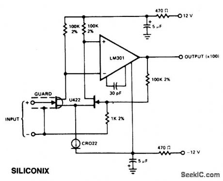
The circuit has an input leakage of only 2 pA typical at 75℃ and would be usable with1 M ohm input resistance. (View)
View full Circuit Diagram | Comments | Reading(668)
CRYSTAL_STABILIZED_IC_TIMER_CANPROVIDE_SUBHARMONIC_FREQUENCIES
Published:2009/7/1 3:59:00 Author:May

View full Circuit Diagram | Comments | Reading(645)
16__to_30_MHz_20_W_SSB_driver_136_V_supply
Published:2009/7/24 3:58:00 Author:Jessie
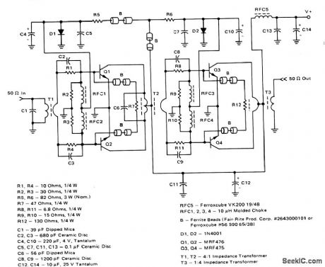
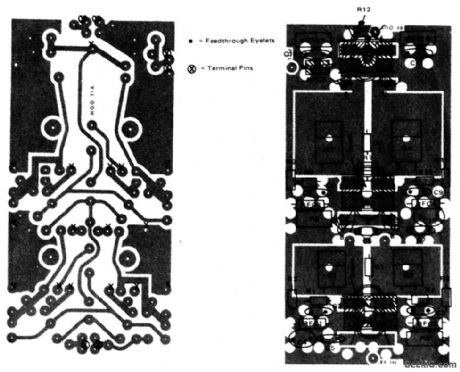
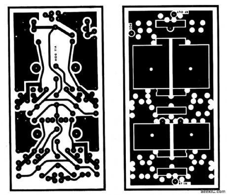
This amplifier provides a total power gain of about 25 dB, and uses inexpensive components (such as plastic RF transistors). The component layout, and PC-board layout, are shown in Figs. 2-55B and 2-55C, respectively. Both the parts and kits for this amplifier are available from: Communications Concepts, 121 Brown St., Dayton, Ohio 45402, (513) 220-9677. (View)
View full Circuit Diagram | Comments | Reading(959)
FET_INPUT_AMPLIFIER
Published:2009/7/1 3:58:00 Author:May
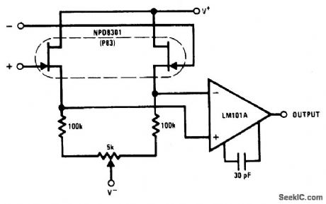
The NPD8301 monolithic-dual provides anideal low offset,low drift buffer function for the LM101A op amp, The excellent matchingcharacteristics of the NPD8301 track well overits bias current range,thus improving common-mode rejection. (View)
View full Circuit Diagram | Comments | Reading(744)
FAST_INDUCTIVE_SWITCHING
Published:2009/7/24 3:58:00 Author:Jessie
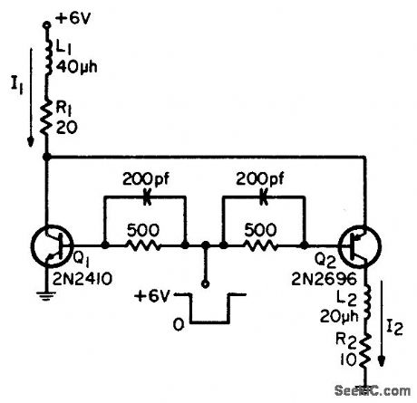
Fast-rise current switching circuit provides current as fast as it can be switched into highly inductive load. Used as current driver for digital com purer memory arrays as well as for speeding up ordinary relays.-T. W. Collins, Fast-Rise Current Switch, FEE, 13:1, p 65-66. (View)
View full Circuit Diagram | Comments | Reading(694)
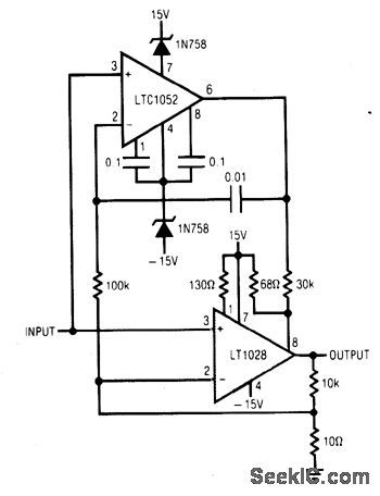
CHOPPER_STABILIZED_AMPLIFIER_
Published:2009/7/1 3:58:00 Author:May
View full Circuit Diagram | Comments | Reading(691)
BATTERY_BACKUP_1
Published:2009/7/1 3:57:00 Author:May
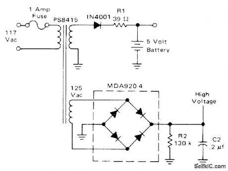
Four nickel-cadmium batteries connected in series provide automatic backup for 5-V supply of digital clock. Under normal AC line operation, battery is continually being recharged with half-wave rectified and unfiltered supply that allows internal chemical reactions to settle between pulses of charging energy. R1 is chosen to make average charging current about 5% of battery rating.-D. Ald-ridge and A. Mouton, Industrial Clock/Time( Featuring Back-Up Power Supply Operation, Motorola, Phoenix, AZ, 1974, AN-718A, p 7. (View)
View full Circuit Diagram | Comments | Reading(854)
CRYSTAL_TESTER
Published:2009/7/1 3:57:00 Author:May
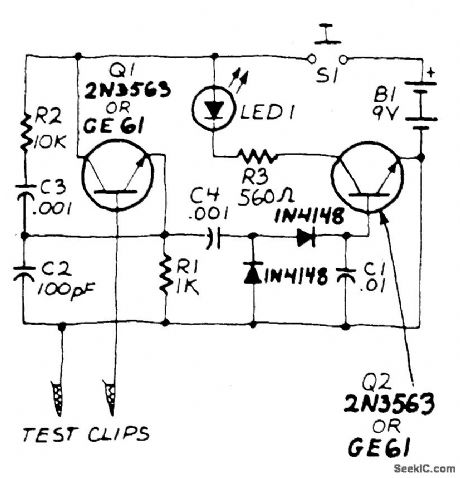
Transistor Q1, a 2N3563, and its associated components form an oscillator circuit that will oscillate if, and only if, a good crystal is connected to the test clips. The output from the oscillator is then rectified by the two 1N4148 diodes and filtered by C1, a.01 μF capacitor.The positive voltage developed across the ca-pacitor is applied to the base of Q2, another 2N3563, causing it to conduct. When that happens, current flows through LED1, causing it to glow. Since only a good crystal will oscillate, a glowing LED indicates that the crystal is indeed Ok. The circuit is powered by a standard nine-volt transistor-radio battery and the SPST pushbutton power-switch is included to prolong battery life. (View)
View full Circuit Diagram | Comments | Reading(0)
Basic_multifunction_regulcttor_application_computer_shutdown
Published:2009/7/24 3:57:00 Author:Jessie
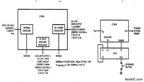
The LT1005 shown here is a multifunction regulator consisting of a 5-V 1-A regulator (controlled by a positive enable signal with a 1.6-V threshold) and a separate 5-V auxiliary regulator. The auxiliary regulator output is unaffected by the main regulator. The LT1005 also includes thermal overload protection and current limiting. The enable pin is a high impedance input which floats in the high state. 10 μA of current pulled from the enable pin shuts down the main output (but not the auxiliary). Figure 9-1B shows a simple, but useful, application. The enable pin is controlled by a toggling flip-flop triggered by a computer keyboard pushbutton. The auxiliary 5-V output powers the FF when the computer is shut down. This eliminates the need for a separate power switch. The enable pin interfaces directly with CMOS or TTL, but the relatively high impedance allows the pin to implement a number of other functions. (View)
View full Circuit Diagram | Comments | Reading(797)
Micropower_precision_reference
Published:2009/7/24 3:57:00 Author:Jessie
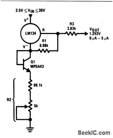
This circuit draws only 10 μA of current. The overall TC of the output will be near zero (less than 50 ppm/°C) when the output is adjusted to 1.253 V by trimming R2. R1 and R2 should track well over temperature. Metal-film resistors with 1% tolerance are recommended. (View)
View full Circuit Diagram | Comments | Reading(746)
ELECTRONIC_R_F_SWITCH
Published:2009/7/24 3:57:00 Author:Jessie
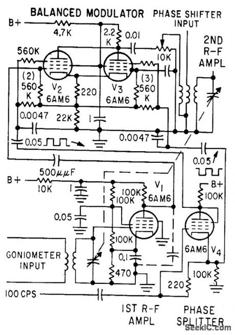
V1 isolates gonio-meter from balanced modulator lubes V2 and V3, which provide 90° phase shift of gonio-meter signal. V2 and V3 are made to conduct alternately by 100-cpsdrive applied to their suppressor grids by phase-splitter V4.-J. F. Hatch and D. W. G. Byatt, Direction Finder with Automatic Readout, Electronics, 32:16, p 52-54. (View)
View full Circuit Diagram | Comments | Reading(707)
4_DIGIT_GAS_DISPLAY
Published:2009/7/1 3:55:00 Author:May
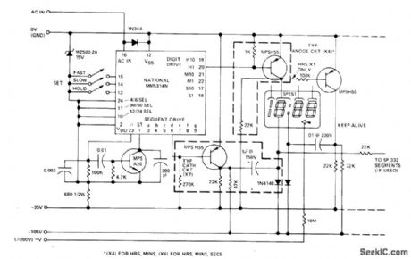
CMOS clock IC drives multidigit gas-discharge display, Simple circuit does not include alarm, flashing colon, and AM/ PM features. Seven segment-driver circuits and four digit-driver circuits are required, although only one of each is shown. Additional drivers are needed if seconds display is desired. Required supply voltages can be obtained from transformer-type supply driving diode bridge;regulation is not needed.-M.S.Robbins, Electronic Clocks and Watches, Howard W.Sans,Indianapolis,IN,1975,p 68-71. (View)
View full Circuit Diagram | Comments | Reading(1260)
HIGH_FREQUENCY_SIGNAL_GENERATOR
Published:2009/7/1 3:54:00 Author:May
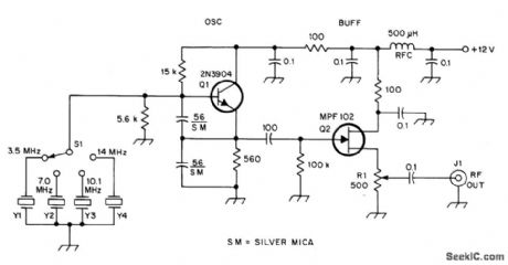
A tapped-coil Colpitts oscillator is used at Q1 to provide four tuning ranges from 1.7 to 3.1 MHz, 3.0 to 5.6 MHz, 5.0 to 12 MHz and 11.5 to 31 MHz. A Zener diode (D2) is used at Q1 to lower the operating voltage of the oscillator. A small value capaci-tor is used at C5 to ensure light coupling to the tuned circuit. Q2 is a source-follower buffer stage. It helps to isolate the oscillator from the generator-output load. The source of Q2 is broadly tuned by means of RFC1. Energy from Q2 is routed to a fed-back, broadband class-A amplifier. A 2 dB attenuator is used at the output of T1 to provide a 50 ohm termination for Q3 and to set the generator-output impedance at 50 ohms.C16, C17 and RFC2 form a brute-force RF decoupling network to keep the generator energy from radiating outside the box on the 12 V supply. (View)
View full Circuit Diagram | Comments | Reading(1503)
SPARK_GAP_SWITCH
Published:2009/7/24 3:56:00 Author:Jessie
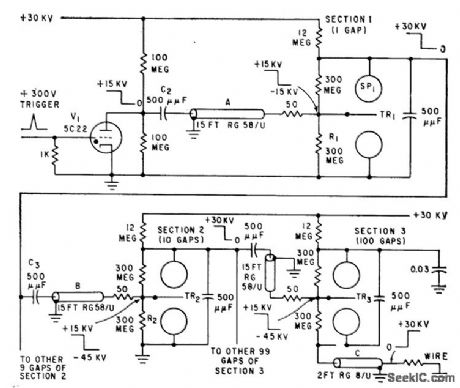
Bank of 111 spark gaps switches 30 kV in less thon 10 millimicrosec, to explode wire for generating plasma in shock tube or generating hypersonic waves in wind tunnel. Jitter problem is solved by using one spark gap to trigger another. Thyratron V1 fires section 1 having single gap, and this triggers 10 gaps in section 2, each of which in turn triggers 10 gaps in section 3.-H. B. McFarlane, Spark Gaps for Fast High-Voltage Switching, Electronics, 32:31, p 72-73. (View)
View full Circuit Diagram | Comments | Reading(1433)
FREQUENCY_TO_VOLTAGE_CONVERTER
Published:2009/7/1 3:52:00 Author:May

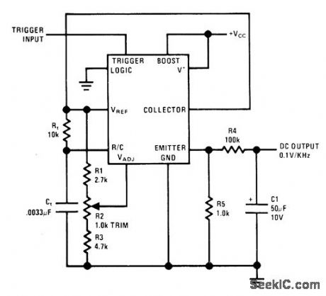
National LM122 timer is used as tachometer by averaging output pulses with simple filter.Pulse width is ad justed with R2 to provideinitialcalibration at 10 kHz. Linearity is about 0.2% foroutput range of 0-1 V. Analog metercan be driven directly by connecting it in series with R5.Supply can range from 4.5 to 40 V.-C. Nelson, Versatile Timer Operates from Microsecondsto Hours, National Semiconductor, Santa Clara, CA, 1973, AN-97, p 10. (View)
View full Circuit Diagram | Comments | Reading(0)
2_INCH_LCD_NUMERALS
Published:2009/7/1 3:52:00 Author:May
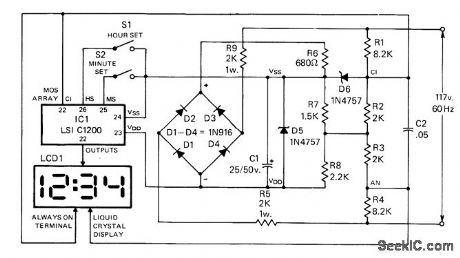
Uses C1200 clock IC made by LSI Computer Systems, having time set, logic, division for seconds, minutes, and hours, 7-segment decoding, and display drivers and switches. Four-digit liquid crystal display panel (LCD) is MGC-50. S1 and S2 advance minutes or hours on display at 2-Hz rate for setting time. To use as elapsed-time indicator, dose S1 and S2 simultaneously to generate reset pulse that sets timing change to zero. When both switches are released simultaneously, time count starts from zero.-R. F. Graf and G. J.Whalen,AGiant LCD Clock, C0, Feb. 1978, p 18-23 and 76. (View)
View full Circuit Diagram | Comments | Reading(1047)
CRYSTAL_CONTROLLED_OSCLLATOR_OPERATES_FROM_ONE_MERCURY_CELL
Published:2009/7/1 3:51:00 Author:May
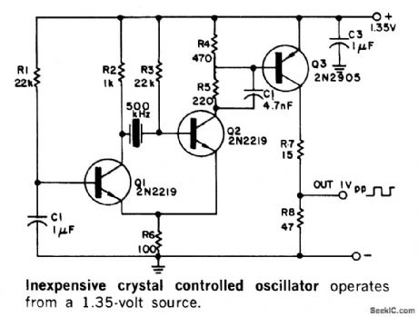
The circuit is powered by a single 1.35 V mercury cell and provides a 1 V squarewave output. As shown, the crystal is a tuned circuit between transistors Q1 and Q2, which are connected in the common-emitter configuration. Positive feedback provided by means of R permits oscillation. The signal at the collector of Q2 is squared by Q3, which switches between cutoff and saturation. R7 permits short-circuit-proof operation. (View)
View full Circuit Diagram | Comments | Reading(975)
FUZZ_BOX_4
Published:2009/7/1 3:49:00 Author:May
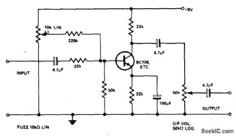
Circuit Notes
None of the components are particularly critical in value or puality ,as distortion is the sole object! The transistor could be BC107-8-9, 2N2926, etc. (View)
View full Circuit Diagram | Comments | Reading(2818)
HIGH_FREQUENCY_CRYSTAL_OSCILLATOR
Published:2009/7/1 3:48:00 Author:May
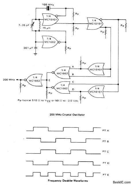
A high speed oscillator is possible by combining an MECL 10 K crystal oscillator with an MECL III frequency doubler as shown. One section of the MC10101 is connected as a 100 MHz crystal oscillator with the crystal in series with the feedback loop. The LC tank circuit tunes the 100 MHz harmonic of the crystal and may be used to calibrate the circuit to the exact frequency. A second section of the MC10101 buffers the crystal oscillator and gives complementary 100 MHz signals. The frequency doubler consists of two MC10101 gates as phase shifters and two MC1662 NOR gates. For a 50% duty cycle at the output, the delay to the true and complement 100 MHz signals should be 90°. This may be built precisely with 2.5 ns delay lines for the 200 MHz output or approximated by the two MC10101 gates. The gates are easier to incorporate and cause only a slight skew in output signal duty cycle. The MC1662 gates combine the 4 phase 100 MHz signals as shown in Figure B. The outputs of the MC1662's are wire-OR connected to give the 200 MHz signal. MECL III gates are used because of the bandwidth required for 200 MHz signals. One of the remaining MC1662 gates is used as a Vgg bias generator for the oscillator. By connecting the NOR output to the input, the circuit stays in the center of the logic swing or at VBB. A 0.001 μF capacitor ensures the VBB circuit does not oscillate. (View)
View full Circuit Diagram | Comments | Reading(0)
STABLE_UNITY_GAIN_BUFFER_WITH_GOOD_SPEED_AND_HIGHINPUT_IMPEDANCE
Published:2009/7/1 3:47:00 Author:May
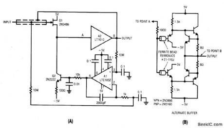
Q1 and Q2 constitute a simple, high speed FET input buffer. Q1 functions as a source follower, with the Q2 current source load setting the drain-source channel current.Normally, this open loop configuration would be quite drifty because there is no dc feedback. The LTC1052 contributes this function to stabilize the circuit by comparing the filtered circuit ot,ttput to a similarly filtered version of the input signal. The amplified difference between these signals is used to set Q2's bias and hence Q1's channel current.This forces Q1's VGS to whatever voltage is required to match the circuit's input and output potentials. The 2000 pF capacitor at A1 provides stable loop compensation. The RC network in Al's output prevents it from seeing high speed edges coupled through Q2's collector-base junction. AZ's output is also fed back to the shield around Q1's gate lead, bootstrapping the circuit's effective input capacitance down to less than 1 pF. For very fast requirements, the alternate discrete component buffer shown will be useful.Although its output is current limited at 75 mA, the GHz range transistors employed provide exceptionally wide bandwidth, fast slewing and very little delay. (View)
View full Circuit Diagram | Comments | Reading(862)
| Pages:1185/2234 At 2011811182118311841185118611871188118911901191119211931194119511961197119811991200Under 20 |
Circuit Categories
power supply circuit
Amplifier Circuit
Basic Circuit
LED and Light Circuit
Sensor Circuit
Signal Processing
Electrical Equipment Circuit
Control Circuit
Remote Control Circuit
A/D-D/A Converter Circuit
Audio Circuit
Measuring and Test Circuit
Communication Circuit
Computer-Related Circuit
555 Circuit
Automotive Circuit
Repairing Circuit