
Circuit Diagram
Index 1181
4_DIGIT_INCANDESCENT
Published:2009/7/1 4:48:00 Author:May

Circuit serves for interfacing CMOS logic to multiplexed 4-digit incandescentdisplay. Scan decoder requires only two input NAND gates since blanking is not required. Incandescentdisplay requires 4.5 V at 24mA per segment when direct-driven; with multiplexing, instantaneous power must be 9 V at 48 mA to maintain same average power per segment. Display protection circuit monitors scan oscillator and blanks display if oscillator fails, to prevent high peak cument from degrading display when applied continuously to 1 digit.-A.Pshaenich, Interface Considerations for Nu-meric Display Systems, Motorola, Phoenix, AZ, 1975, AN-741, p 25. (View)
View full Circuit Diagram | Comments | Reading(846)
BIDIRECTIONAL_MONO
Published:2009/7/1 4:47:00 Author:May
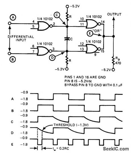
Requires only one IC, three resistors, and one capac;tor. WilI trigger on both positive- and negative-going transi-tions, as required in critical timing applications Involving pulses narrowerthan 50 ns. Capacitor altemately discharges through one pulldown resistor to threshold, then the other. Output gates are tied together to form common output.Width of pulse is defined by values of components.-W. A. Palm Bidirectional ECL One-Shot Uses a Single IC. EDN Magazine. Jan. 5. 1977. p 41-42. (View)
View full Circuit Diagram | Comments | Reading(668)
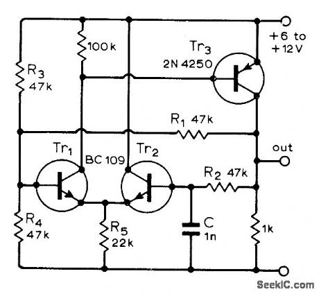
AUTOMATIC_BRIGHTNESS_CONTROL
Published:2009/7/1 4:44:00 Author:May
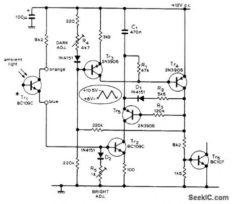
Circuit adjusts brightness of LED digital display by altering mark-space ratio of LED supply voltage.Ambient-light input is sensed by BC109C transistor with top taken off. Normal display current of 20 mA is reduced to 2 mA when darkened room makes brightness unnecessary, conserving battery life. Tr3 and Tr4 operate as Schmitt trigger, with mark time of 1.5 ms determined by R2 and space time controlled by charging current through Tr5 and Tr2 as affected by ambient light on Tr1. Article gives complete circuits for driving 11-LED array. To add brightness control circuit, break ground connection of LED supply transistors and insert saturated transistor Tr6.-G. Kalanit, Analogue to Digital Meter, Wireless World, July 1976, p 53-57.
(View)
View full Circuit Diagram | Comments | Reading(0)
16_to_30_MHz_20_W_SSB_driver_28_V_supply
Published:2009/7/24 4:03:00 Author:Jessie
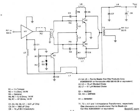
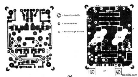
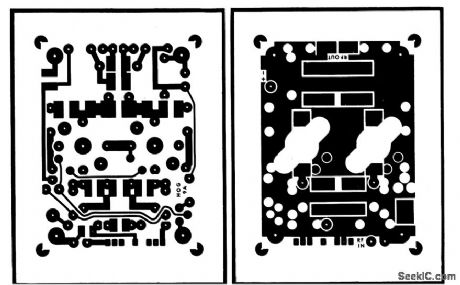
This amplifier provides a total power gain of about 55 dB, and is a 28-V vers1on of the circuit in Fig.2-55 The component layout,and PC-board layout, are shown in Figs.2-56B and 2-56C,respectively,Both the parts and kits for this amplifier are available from∶Communications concepts,121 Brown St, Dayton、Ohio45402(513)220-9677 (View)
View full Circuit Diagram | Comments | Reading(755)
PULSE_WIDTH_PROPORTIONAL_CONTROLLER_CIRCUIT
Published:2009/7/1 4:42:00 Author:May
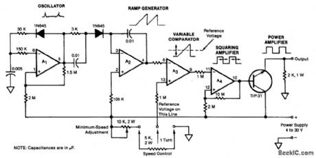
The quad operational amplifier circuit yields full 0 to 100 percent pulse-width control.The controller uses an LM3900 that requires only a single supply voltage of 4 to 30 V.The pulse-repetition rate is set by a 1 kHz oscillator that incorporates amplifier A1. The oscillator feeds ramp generator A2, which generates a linear ramp voltage for each oscillator pulse. The ramp signal feeds the inverting input of comparator A3; the speed-control voltage feeds the noninverting input. Thus, the output of the comparator is a 1 kHz pulse train, the pulse width of which changes linearly with the control voltage.The control voltage can be provided by an adjustable potentiometer or by an external source of feedback information such as a motor-speed sensing circuit. Depending on the control-voltage setting, the pulse duration can be set at any value from zero (for zero average dc voltage applied to the motor) to the full pulse-repetition period (for applied motor voltage equal to dc power-supply voltage). An amplifier stage (A4) with a gain of 10 acts as a pulse-squaring circuit. A TIP-31 medium-power transistor is driven by A4 and serves as a separate power-amplifier stage. (View)
View full Circuit Diagram | Comments | Reading(2014)
554_M0N0
Published:2009/7/1 4:41:00 Author:May
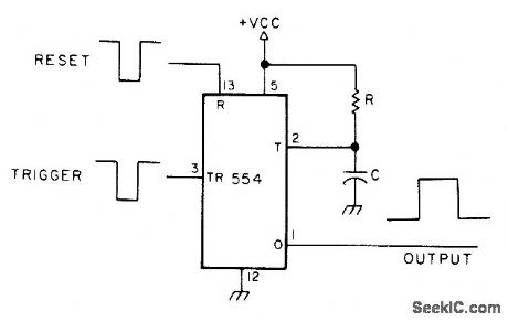
Uses one section of 554 quad monostable timer, connected to give output pulse for negative-going trigger pulse. Width of output pulse in seconds is equal to RC. Trigger must be narrower than output pulse. VCC is 4.5-16 V at 3-10 mA.-H. M. Berlin. IC Timer Review. 73 Magazine, Jan. 1978. p 40-45. (View)
View full Circuit Diagram | Comments | Reading(600)
SOLID_STATE_SWITCHING
Published:2009/7/24 4:02:00 Author:Jessie
Used in high-speed data transmission system having 15-gc bandwidth. Use of Kita diodes gives transition lime of 20 nsec for break and 40 nsec for restoration, pg compared to 1 millisec for reed relays.-I. Someya, Bidding For World Leadership in Solid State Micro. wave Gear, Electronics, 38:25, p 99-105. (View)
View full Circuit Diagram | Comments | Reading(770)
TOSS_A_COIN_BINARY_BOX
Published:2009/7/1 4:40:00 Author:May
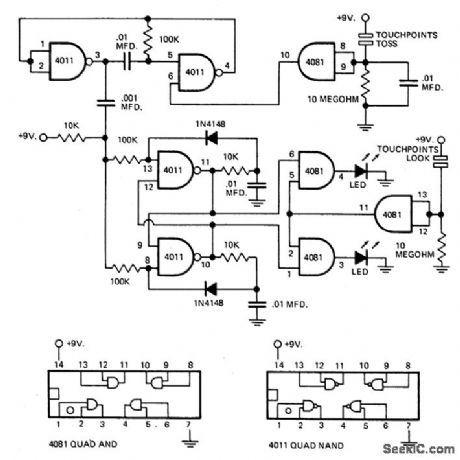
Circuit NotesCircuit uses an astable multivibrator to vary the heads-or-tails condition, and a flip-flop that the flip-flop's state is changed once for to store the condition given by the multivieach full cycle the multivibrator goes through to assure an absolutely even 50-50 chance of a brator. Consequently, the circuit is wired so heads or tails loss. (View)
View full Circuit Diagram | Comments | Reading(889)
DUAL_5_V_SUPPLY
Published:2009/7/24 4:02:00 Author:Jessie
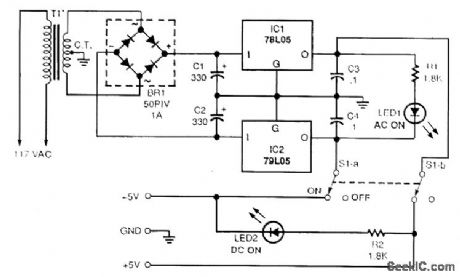
This is a circuit for a simple dual 5-V supply for experimental use. T1 is a 12-V center-tapped 0.3-A transformer. (View)
View full Circuit Diagram | Comments | Reading(794)
FOUR_GATE_MONO
Published:2009/7/1 4:38:00 Author:May
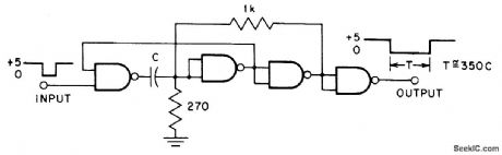
NAND-gate mono using Texas Instruments SN7400 package provides cleaner, more stable output. Feedback resistor eliminates tendency to oscillate. Output pulse width T is equal to 1.3 RC; when R is 270 ohms,T is 350 C. Input pulse widths over 30 ns can initiate output. C can be 100 pF to 100 μF.-J.E. McAlister, Single NAND Package Improves One-Shot, EEE Magazine. Aug. 1970. p 78. (View)
View full Circuit Diagram | Comments | Reading(636)
Flybctck_regulator_with_low_quiescent_current
Published:2009/7/24 4:02:00 Author:Jessie
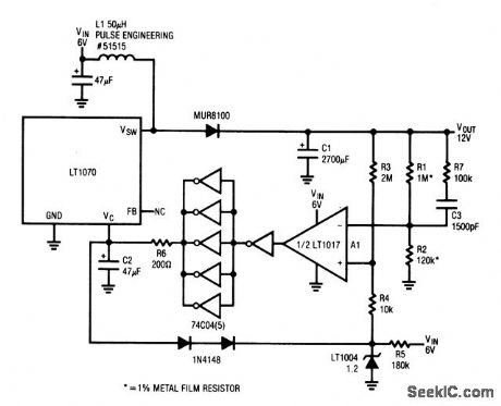
The quiescent current of this flyback regulator is a low 150 μA- even though the circuit is capable of delivery a maximum of 2 A at 12 V. (View)
View full Circuit Diagram | Comments | Reading(670)
GAME_ROLLER_OR_CHASE_CIRCUIT
Published:2009/7/1 4:34:00 Author:May
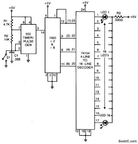
Circuit NotesThe 555 timer produces a rapid series of pulses whenever switch S1 is open. These pulses are counted in groups of 16 and con-verted into binary form by the 7493 and applied to the 74154 (a 1-of-16 decoder/demultiple xer) wired so that each of its 16 output lines goes low sequentially and in step with the binary count delivered by the 7493. When the switch is closed, only one LED remains on. 0nly one current limiting resistor (R3) is used for all the LED's since only one is on at any one time. (View)
View full Circuit Diagram | Comments | Reading(3323)
PUNCH_PRESS_SAFETY_SWITCH
Published:2009/7/24 4:02:00 Author:Jessie
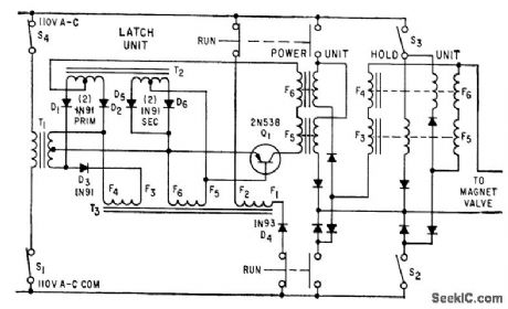
Static switching control for dangerous presses requires that both hands of operator be on run push buttons, out of danger area, before ram can descend. To prevent operators from jamming or taping one or more buttons closed, control circuit stops press at end of cycle. Both buttons must then be released and depressed again to start new cycle. self-exched magnetic amplifier operates much like snap switch.-S. A. Zarleng, Static Switching Techniques for Machine-Tool Safety, Electronics, 32:24, p 57-59. (View)
View full Circuit Diagram | Comments | Reading(861)
PICOAMMETER_CIRCUIT
Published:2009/7/1 4:32:00 Author:May
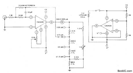
The circuit uses the exceptionally low input current (0.1pA) of the CA3420 BiMOS op amp. With only a single 10 megohm resistor, the circuit covers the range from ± 50 pA maximum to a full-scale sensitivity of ± 1.5 pA. Using an additional CA3420, a low-resistance center tap is obtained from a single 3-volt lithium battery. (View)
View full Circuit Diagram | Comments | Reading(1884)
MISSILE_COUNT_DOWN_SWITCH
Published:2009/7/24 4:01:00 Author:Jessie
Level-sensitive switch uses nonlinear negative feedback to provide stable operation (within 1.5%) over 100℃ temperature range. Monostable mvbr is followed by rectifying transistor and filter. For signals above trigger level, circuit is periodically switched into its transient stale.-D. W. Boensel, Switching Circuits for Missile Count-Downs, Electronics, 32;31, p 76-78. (View)
View full Circuit Diagram | Comments | Reading(654)
20_kHz_ASTABLE
Published:2009/7/1 4:32:00 Author:May
Single-capacitor circuit is reIiable over wide range of temperatures. voltages. and transistor gains. Frequency varies only by 0.05% for supply voltage changes between 6 and 12 V. Timing can be changed with R1. R2. and C. Ducy cycle depends on ratio of R3. to R4. and is 50% forvaluesshown.-C. Horwitz, Tolerant Astable Circuits. Wireless World. Feb.1975,p93. (View)
View full Circuit Diagram | Comments | Reading(852)
15__to_5_V_converter_with_200_mA_output
Published:2009/7/24 3:56:00 Author:Jessie
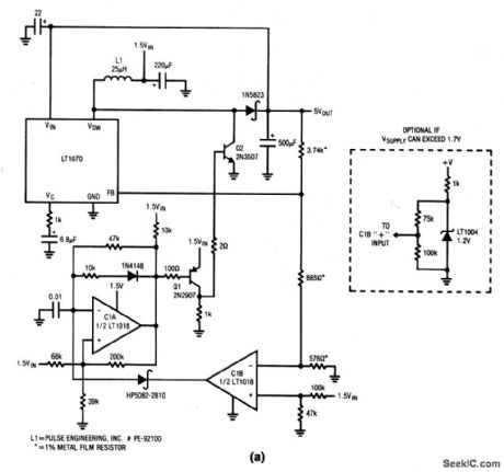
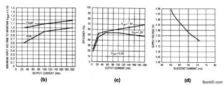
This circuit also converts 1.5 V to 5 V, but with higher output current and quiescent current than the circuit of Fig. 8-47. Figures 8-48B, 8-48C, and 8-48D show the characteristics. (View)
View full Circuit Diagram | Comments | Reading(717)
AUTOMATIC_LEVEL_CONTROL
Published:2009/7/1 4:31:00 Author:May
The NE570 can be used to make a very high performance ALC compressor, except that the rectifier input is tied to the input. This makes gain inversely proportional to input level so that a 20 dB drop in input level will produce a 20 dB increase in gain. The output will remain fixed at a constant level. As shown, the circuit wilt maintain an output level of ±1 dB for an input range of +14 to -43 dB at 1 kHz. Additional external components will allow the output level to be adjusted. (View)
View full Circuit Diagram | Comments | Reading(838)
AUDIO_Q_MULTIPLIER
Published:2009/7/1 4:30:00 Author:May
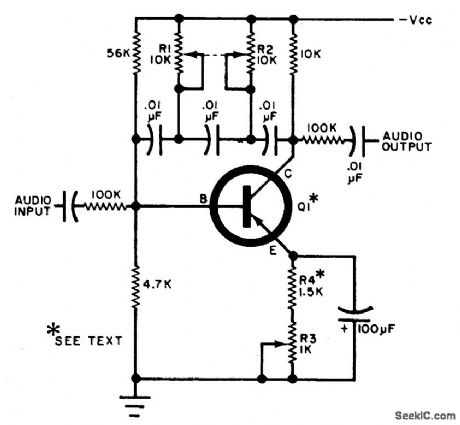
This circuit is for selective tuning between two closely spaced audio tones. The selective frequency is dependent on the value of capacitors and resistors in the feedback circuit between the collector and base of Q1. With the values shown, the frequency can be tuned a hundred cycles or so around 650 Hz. RI and R2 must be ganged. Emitter potentiometer R3 determines the sharpness of response curve. Any transistor having a beta greater than 50 can be used. Select a value for R4 so that the circuit will not oscillate when R3 is set for minimum bandwidth (sharpest tuning). (View)
View full Circuit Diagram | Comments | Reading(1143)
HIGH_INPUT_IMPEDANCE_DIFFERENTIAL_AMPLIFIER
Published:2009/7/1 4:29:00 Author:May
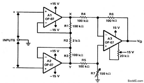
Operational amplifiers A1 and A2 are connected in a non-inverting configuration with their outputs driving amplifier A3. Operational amplifier A3 could be called a subtractor circuit which converts the differential signal floating between points X and Y into a singleended output voltage. Although not mandatonr,_amplifier A3 is usually operated at unity gain and R4, R5, R6, and R7 are all equal.The common-mode-rejection of amplifier A3 is a function of how closely the ratio R4:R5 matches the ratio R6:R7. For example, when using resistors with 0.1% tolerance, common-mode rejection is greater than 60 dB. Additional improvement can be attained by using a potentiometer (slightly higher in value than R6) for R7. The potentiometer can be adjusted for the best common-mode rejection. Input amplifiers Al and A2 will have some differential gain but the common-mode input voltages will experience only unity gain. These voltages will not appear as differential signals at the input of amplifier A3 because, when they appear at equal levels on both ends of resistor R2, they are effectively canceled.This type of low-level differential amplifier finds widespread use in signal processing.It is also useful for dc and low-frequency signals commonly received from a transducer or thermocouple output, which are amplified and transmitted in a single-ended mode.The amplifier is powered by ±15 V supplies. It is only necessary to null the input offset voltage of the output amplifier A3. (View)
View full Circuit Diagram | Comments | Reading(1760)
| Pages:1181/2234 At 2011811182118311841185118611871188118911901191119211931194119511961197119811991200Under 20 |
Circuit Categories
power supply circuit
Amplifier Circuit
Basic Circuit
LED and Light Circuit
Sensor Circuit
Signal Processing
Electrical Equipment Circuit
Control Circuit
Remote Control Circuit
A/D-D/A Converter Circuit
Audio Circuit
Measuring and Test Circuit
Communication Circuit
Computer-Related Circuit
555 Circuit
Automotive Circuit
Repairing Circuit