
Circuit Diagram
Index 1197
LINEAR_FREQUENCY_METER(AUDIO_SPECTRUM)
Published:2009/7/1 2:24:00 Author:May
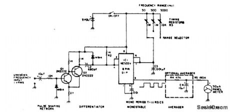
Circuit NotesThe 555 is used in a monostable multivibrator circuit that puts out a fixed timewidth pulse, which is triggered by the unknown input frequency. (View)
View full Circuit Diagram | Comments | Reading(763)
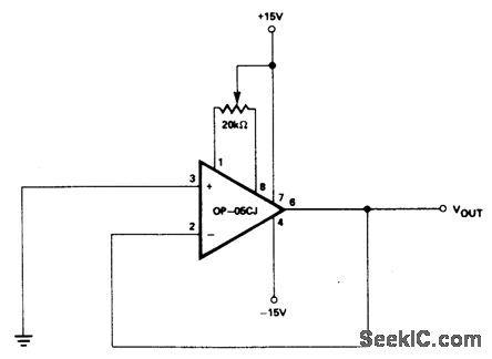
High_stability_voltage_reference
Published:2009/7/24 5:15:00 Author:Jessie


This circuit provides a precision voltage reference without the use of an IC voltage reference. (View)
View full Circuit Diagram | Comments | Reading(1422)
METAL_LOCATOR_Ⅱ
Published:2009/7/1 2:23:00 Author:May

The circuit consists of two oscillators, both working at about 465 kHz. One uses an if transformer and the other uses an inductor (the search coil L1). The oscillators are coupled by a capacitor (10 pF). A beat note (produced if the two oscillators are working closely together) is detected by the diode and fed to the headphone amplifier and the 22μF capacitor. The search coil oscillator is tuned by a 10-365 pf variable capacitor.The search coil comprises 22 turns of wire (any gauge between 24 swg and 36 swg enamel) center tapped. The wire should be wound on a temporary form then taped and glued to a piece of hardboard. The coil size should be about 6 x 6 . Headphones should be high impedance. (View)
View full Circuit Diagram | Comments | Reading(1520)
Thermally_based_NiCad_charger_with_low_imynedance_charging_source
Published:2009/7/24 5:15:00 Author:Jessie

Figure 8-19 shows a thermally based NiCad charger operated in the switching mode. The circuits of Figs. 8-15 and 8-18 both force the transistor to dissipate some power, and the resulting heat might be a problem in a small enclosure (typical of micropower circuits). The circuit of Fig. 8-19 relies on the source impedance of the wall transformer to limit current through Q1 and the battery pack. The source impedance can be set when specifying the transformer. LINEAR TECHNQLOGY, APPLICATION NOTE 37, P. 3. (View)
View full Circuit Diagram | Comments | Reading(631)
ac_power_fail_and_brownout_detector
Published:2009/7/24 5:08:00 Author:Jessie

This circuit detects ac undervoltage by monitoring the secondary side of the transformer with an ICL7665S(Fig.9-15B).C1 is charged through R1 when OUT1 is off.With a nominal 110 V input to the transformer,OUT1 discharges C1once every cycle(about every 16.7 ms).When the ac input voltage is reduced,OUT1 stays off so that C1 does not discharge.When the voltage on C1 reaches 1.3V,OUT2 turns off,and the power-fail warning goes high.The R1C1 time constant is chosen so that it takes longer than 16.7 ms to charge C1 to 1.3 V. (View)
View full Circuit Diagram | Comments | Reading(1470)
±_3_V_REFERENCE
Published:2009/7/1 2:23:00 Author:May

View full Circuit Diagram | Comments | Reading(580)
ZENERLESS_PRECISION_MILIVOLT_SOURCE
Published:2009/7/1 2:22:00 Author:May
View full Circuit Diagram | Comments | Reading(784)
Low_noise_chopper_stabilized_bridge_amplifier
Published:2009/7/24 5:07:00 Author:Jessie
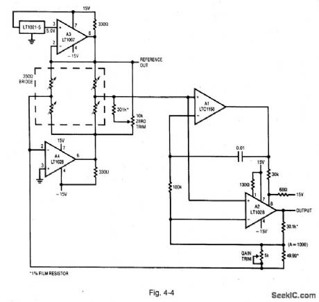
Figure 4-4 shows a circuit that is similar to that of Fig. 4-3, except that A1 is chopper stabilized. This reduces the offset error even further. A1 measures the dc error at the A2 inputs and biases the A1 offset pins to force an offset of a few microvolts. The offset-pin bias at A2 is arranged so that A1 will always be able to find the servo point.The 0.01-μF capacitor rolls off A1 at low frequencies, with A2 handling the high-frequency signals. Returning the A2 feedback string to the bridge midpoint eliminates the A4 offset contribution. If this was not done, A4 would require a similar offset-correction loop. The circuit has a drift of less than 0.05-μV/℃, 1-nV/Hz noise, and CMRR exceeding 160 dB. LINEAR TECHNOLOGY, APPLICATION Nom 43, P. 6. (View)
View full Circuit Diagram | Comments | Reading(771)
MEDICAL_INSTRUMENT_PREAIVIPLIFIER
Published:2009/7/1 2:22:00 Author:May
Note that AVOL=25; single Ni-cad battery operation. Input current (from sensors connected to the patient) is limited to less than 5μh under fault conditions. (View)
View full Circuit Diagram | Comments | Reading(617)
Low_noise_bridge_amplifier_with_common_mode_suppression
Published:2009/7/24 5:06:00 Author:Jessie
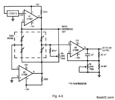
Figure 4-3 shows a circuit that is similar to that of Fig. 4-2, except that low-noise bipolar amplifiers are used. This circuit trades slightly higher dc offset drift for lower noise; it is a good candidate for stable resolution of small, slowly varying measurements. LINEAR TECHNOLOGY, APPLICATION NOTE 43, P. 6. (View)
View full Circuit Diagram | Comments | Reading(901)
12_V_AUTO_CLOCK
Published:2009/7/1 2:21:00 Author:May

National MA1003 automotive/instrument clock module combines MM5377 MOS LSI clock with 4-digit 0.3-inch green vacuum fluorescent display,2.097-MHz crystal, and discrete components on single printed-circuit board to give complete digital clock. Brightness control logic blanks display when ignition is off, reduces brightness to 33% when parking or headlight lamps are on, and follows dash-lamp dimming control setting.Display has leading- zero blanking. For portable applications, display can be activated by closing display switch momentarily,- MOS/LSI Data-book, National Semiconductor, Santa Clara, CA, 1977, p 13-8-13-10.
(View)
View full Circuit Diagram | Comments | Reading(5499)
HIGH_STABILITY__VOLTAGE_REFERENCE
Published:2009/7/1 2:21:00 Author:May
View full Circuit Diagram | Comments | Reading(638)
Servo_controlling_bridge_drive
Published:2009/7/24 5:05:00 Author:Jessie
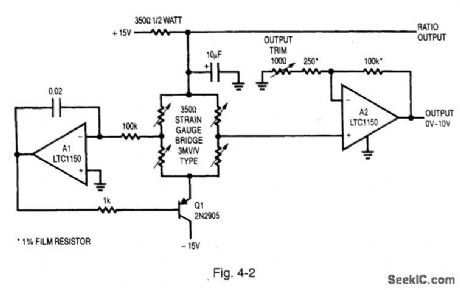
Figure 4-2 shows a way to reduce errors because of the bridge common-mode output voltage. A1 biases Q1 to servo the bridge left midpoint to zero under all operating conditions. The 350-Ω resistor ensures that A1 will find a stable operating point with 10 V of drive delivered to the bridge. This allows A2 to take a single-ended measurement, eliminating all common-mode voltage errors. LINEAR TECHNOLOGY, APPLICATION NOTE 43, P. 5. (View)
View full Circuit Diagram | Comments | Reading(861)
HEART_RATE_MONITOR
Published:2009/7/1 2:21:00 Author:May

Light filtering through the finger tip is detected by the cadmium sulphide photoresistor CD1 which forms the feedback network for transducer amplifier section ICA producing a weak signal which is further amplified by ICB. This signal is now compared against a user adjusted threshold, comparator ICD triggers gating on the piezoelectric buzzer PZ1. On each falligg edge of the comparator's output signal one-shot multivibrator ICD produces a 2 μs pulse which is inverted by Q1 and averaged by the RC network consisting of Ml, C6 and C7. The 10 K trimpot R20 in Q1's collector circuit sets the scale factor for M: where full scale is 150 beats per minute. (View)
View full Circuit Diagram | Comments | Reading(27)
Bridge_based_instrumentation_amplifier
Published:2009/7/24 5:04:00 Author:Jessie
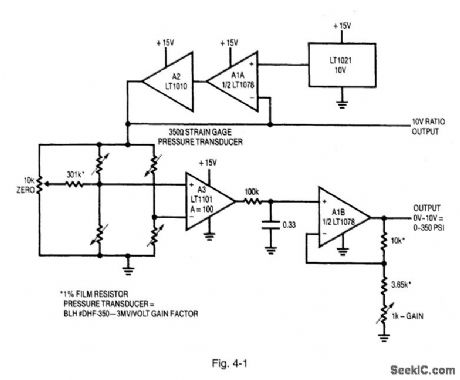
Figure 4-1 shows signal conditioning for a 350-Ω transducer bridge. The specified strain-gauge pressure transducer produces 3-mV output per volt of bridge excitation. The LT1021 reference, buffered by A1A and A2, drives the bridge. This potential also supplies the ratio output, permitting radiometric operation of a monitoring analog-to-digital converter (Chapter 8). Amplifier A3 extracts the bridge differential output at a gain of 100, with additional trimmed gain supplied by A1B. The circuit shown can be adjusted for a precise 10-V output at full-scale pressure. To trim the circuit, apply zero pressure to the transducer, adjust the 10-kΩ pot until the output just comes off 0 V. Then apply full-scale pressure and trim the 1-kΩ adjustment. Repeat the procedure until both points are fixed. LINEAR TECHNOLOGY, APPLICATION NOTE 43, P. 5. (View)
View full Circuit Diagram | Comments | Reading(1205)
Power_fail_warning_and_power_up_power_down_reset
Published:2009/7/24 5:01:00 Author:Jessie

When the unregulated dc input of this circuit is above the trip point, OUT1 is low. When the dc input drops below the trip point, OUT1 shuts off and the power-fail warning goes high. The voltage on the input of the 7805 decays at a rate of IOUT/C. Because the 7805 continues to provide a 5-V output at 1 A until VIN is less than 7.3v, this circuit provides a certain amount of warning before the 5-V output begins to drop. The ICL7665S OUT2 (Fig. 9-15B) is used to prevent a microprocessor from writing spurious data to a CMOS battery-backup memory by causing OUT2 to go low when the 7805 5-V output drops below the ICL7665S trip point. (View)
View full Circuit Diagram | Comments | Reading(1318)
UNIDIRECTIONAL_MOTION_SENSOR
Published:2009/7/1 2:19:00 Author:May

This circuit detects an object passing in one direction but ignores it going the opposite way. Two sensors define the sense of direction. The object blocks the light to phototransistor Q1 or Q2 first dependent on the direction of approach. When the object passes Q1 then Q2, an output pulse is generated at D; while no pulse is seen at D as the object passes Q2 then Q1. Object length (measured along the direction of the two sensors) should be greater than the separation of the two sensors Q1 and Q2. (View)
View full Circuit Diagram | Comments | Reading(1285)
Chopper_stabilized_comparator
Published:2009/7/24 4:58:00 Author:Jessie

Fig. 15-39 This circuit uses an LTC1043 (Fig. 1-4B) to stabilize a high-speed low-drift comparator. The circuit is applicable only in situations where some dead time is available for zeroing action to occur. Comparator offset is well within 5μV, with negligible temperature drift. Notice that the status output (pin 3) should be used to indicate the circuit operating state, rather than the zero command (pin 16), because the status-output timing includes the 50-ns delay of the LTC1043 switch. Linear Technology Linear Applications Handbook 1990, p. AN9-11. (View)
View full Circuit Diagram | Comments | Reading(1101)
QUARTZ_MOTOR_WRISTWATCH
Published:2009/7/1 2:19:00 Author:May
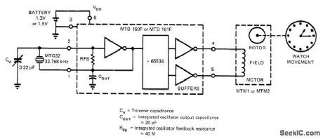
Uses one 32.768-kHz crystal at input of Motorola MTD 160F or 161F custom CMOS chip,Mith stepper motor at output of chip fordriving conventional watch hands. Chip contains three-inverter oscillator, 16 counting flip-flops, and motor drive buffers.-B. Furlow, CMOS Gates in Linear Applications: The Results Are Surprisingly Good, EDN Magazine, March 5, 1973, p 42-48. (View)
View full Circuit Diagram | Comments | Reading(816)
MAKING_SLOW_LOGIC_PULSES_AUDIBLE
Published:2009/7/1 2:18:00 Author:May
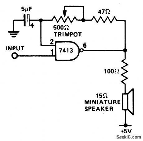
This circuit is useful for monitoring slow logic pulses as a keying monitor or digital clock alarm. The Schmitt trigger is connected as an oscillator. The trimpot controls the pitch of the output. When the input goes high, the circuit will oscillate. (View)
View full Circuit Diagram | Comments | Reading(631)
| Pages:1197/2234 At 2011811182118311841185118611871188118911901191119211931194119511961197119811991200Under 20 |
Circuit Categories
power supply circuit
Amplifier Circuit
Basic Circuit
LED and Light Circuit
Sensor Circuit
Signal Processing
Electrical Equipment Circuit
Control Circuit
Remote Control Circuit
A/D-D/A Converter Circuit
Audio Circuit
Measuring and Test Circuit
Communication Circuit
Computer-Related Circuit
555 Circuit
Automotive Circuit
Repairing Circuit