
Circuit Diagram
Index 1189
555_ASTABLE_WITH_LOW_DUTY_CYCLE
Published:2009/7/1 2:43:00 Author:May
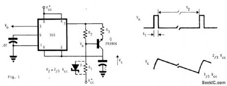
This free-running multivibrator uses an external current sink to discharge the timing capacitor, C. Therefore, interval t2 may easily be 1000 x the pulse duration, t1, which defines a positive output. Capacitor voltage, VC, is a negative going ramp with exponential rise during the pulse output periods. (View)
View full Circuit Diagram | Comments | Reading(764)
SENSITIVE_A_C_POWER_SWITCH
Published:2009/7/24 4:12:00 Author:Jessie
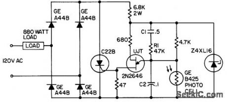
Used to switch load in response to gradually changing signal, as from photocell or thermistor.Provides snap-action switching from full on to full oil, with differential between switching conditions adjustable over wide range by changing C1 and R1.- Transistor Manual, Seventh Edition, General Electric Co., 1964, p 331. (View)
View full Circuit Diagram | Comments | Reading(796)
6_DIGIT_DISPLAY
Published:2009/7/1 2:41:00 Author:May

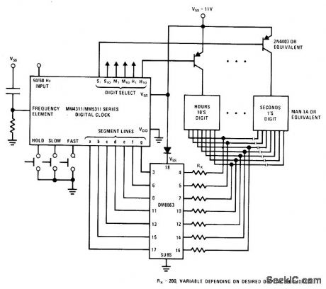
National DM8863 8-digit LED drivel serves as segment dlver for common-anode display of hours,minutes,and seconds,replacing total of 14 resistors and 7 transistors.-C. Carinalli, Driving 7-Segment LED Displays with National Semiconductor Circults, National Semiconductor, Santa Clara,CA,1974,AN-99,p 11. (View)
View full Circuit Diagram | Comments | Reading(1053)
Electrostatic_transducer_for_ultrasonic_measurement
Published:2009/7/24 4:11:00 Author:Jessie
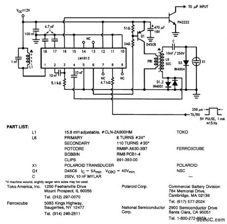
Pig. 14-23 The LM1812 is a complete ultrasonic transceiver used in a variety of pulse/echo-ranging applications. In this circuit, the LM1812 transmits a burst of oscillations with transducer X1. Then, using the same X1, listens for a return echo. If an echo of sufficient amplitude is received, the LM1812 detector produces a pulse (pin 16) of about the same width as the original burst. The closer the reflecting object, the earlier the return echo. Using the values and parts shown, the circuit has a range of about 4 inches to 30 feet. L6 resonates at 50 to 60 kHz, with the 500-pF capacitance of X1. L1 is tuned to this frequency by watching for maximum echo sensitivity with a scope at pin 1. National Semiconductor. Linear Applications Handbook 1991. p. 1173. (View)
View full Circuit Diagram | Comments | Reading(2742)
PRECISION_REFERENCE_STANDARD_CELL_REPLACEMENT
Published:2009/7/1 2:40:00 Author:May
View full Circuit Diagram | Comments | Reading(633)
Four_cell_NiCad_regulator_charger
Published:2009/7/24 4:11:00 Author:Jessie
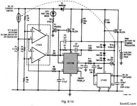
Figure 8-14 Shows an LTC1155 dual-power MOSFET driver connected to providecontrol of a four-cell charger/regulator. The LTC1155 has the ability to deliver 12-V of gate drive to two N-channel power MOSFETs when powered from a 5-V supplywith no external component required, The circuit is suited for a notebook-computer supply.(A four-cell NiCad battery pack can be used to power a 5-Vnotebook computer.)Q3 and Q4 must be provided with heatsinks.The regulator ISswitched off by the microprocessor when the battery voltage drops below 4.6V The standby current for the 5-V 2-A regulator is less than 10 μA.The regulator is switched on agam when the battery voltage rlses during charging. LINEAR TECHNOLOGY, DESIGN NOTE 51 P.1
(View)
View full Circuit Diagram | Comments | Reading(984)
NR_DIODE_AS_BISTABLE_SWITCH
Published:2009/7/24 4:11:00 Author:Jessie
Bonded negative-resistance diode switches to high-current stale on arrival of first pulse. Pulse is shut off before capacitor current through diode falls below negative spike on trailing edge of pulse.-A. P. Schmid, Jr., Negative. Resistance Diode Handles High Power, Electronics, 34:34, p 44-46. (View)
View full Circuit Diagram | Comments | Reading(712)
NEON_LAMP_CAPACITOR_DISCHARGER
Published:2009/7/24 4:10:00 Author:Jessie
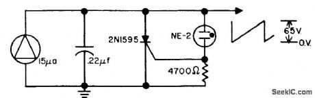
Used to discharge capacitor being charged from constant-current source providing about 15 microamp. Circuit has extremely high impedance until breakdown, then low enough impedance to discharge capacitor to fraction of volt.-R. W. Biddlecomb, High-Current Switch Has High ON/OFF Z Ratio, EEE, 12:2, p 29. (View)
View full Circuit Diagram | Comments | Reading(861)
Fluid_level_control_system
Published:2009/7/24 4:10:00 Author:Jessie

Pig. 14-22 This circuit shows a simple system to control the emptying or filling process of a fluid container. The only transducers or probes involved are stainless-steel screws and hook-up wire (Fig. 14-22B). The fluid is drained by a motor-operated pump, which, in turn, is controlled by relay RY1. When the system is connected, as shown in Fig. 14-22A (for a sump or bilge pump), the pump motor (typically, a 1/4 HP) operates when the fluid level reaches the start probe, and continues until the level reaches the stop level. If the system is to control the filling process, use the circuit of Fig. 14-22C, National Semiconductor Linear Applications Handbook, 1991, p. 1169. (View)
View full Circuit Diagram | Comments | Reading(773)
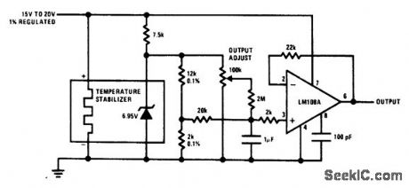
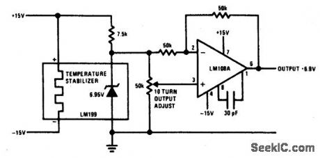
PRECISION_REFERENCE_O_V_TO_20_V_POWER_REFERENCE
Published:2009/7/1 2:39:00 Author:May
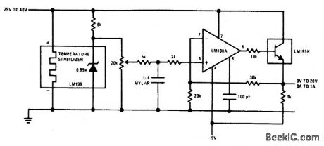
View full Circuit Diagram | Comments | Reading(665)
SATURABLE_REACTOR_LATCH
Published:2009/7/24 4:09:00 Author:Jessie
Offers operating simplicity, high speed, and low cost. Transistor model can switch in less than 0.5 microsec. Current through N1, when V1 conducts, saturates core of T1.-W. J. Reap, Simple Latch Circuit Uses Saturable Reactor, Electronics, 33:2, p 66. (View)
View full Circuit Diagram | Comments | Reading(675)
RAMP_GENERATOR_WITH_VARIABLE_RESET_LEVEL
Published:2009/7/1 2:39:00 Author:May
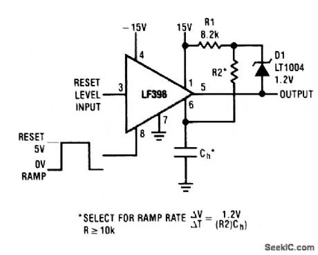
View full Circuit Diagram | Comments | Reading(1362)
DC_10_kHz_FREQUENCY_VOLTAGE_CONVERTER
Published:2009/7/1 2:39:00 Author:May
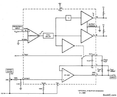
Circuit Notes
The converter generates an output vol-tage which is linearly proportional to the input frequency waveform. Each zero crossing at the comparator's input causes a precise amount of change to be dispensed into the op amp's sum-ming junction. This charge in turn flows through the feedback resistor generating voltage pulses at the output of the op amp.Capacitor (CINT) across Rtxt averages these pulses into a dc voltage which is linearly proportional to the input frequency. (View)
View full Circuit Diagram | Comments | Reading(0)
PRECISION_REFERENCE_BIPOLAR_OUTPUT_REFERENCE
Published:2009/7/1 2:39:00 Author:May
View full Circuit Diagram | Comments | Reading(752)
PRECISION_DUAL_TRACKING_VOLTAGE_REFERENCES
Published:2009/7/1 2:38:00 Author:May
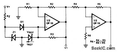
View full Circuit Diagram | Comments | Reading(739)
High_performance_isolation_amplifier
Published:2009/7/24 4:09:00 Author:Jessie
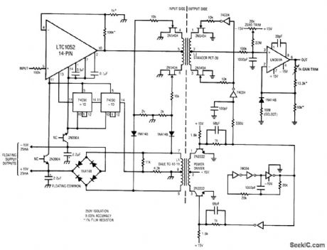
Fig. 14-21 This amplifier features inputs, which are galvanically isolated from the output and power connections, as required by many factory and process-control environments. The isolation allows this amplifier to ignore the effects of transducer ground loops, and operate at input common-mode voltages many times the power-supply voltage. The circuit has a 0.03% transfer accuracy, a 50-nV/℃ input drift, a gain of 1000, and will operate at 250-V input common-mode levels. To trim, tie the A1 input to floating common and adjust the zero trim for 0-V output. Next, connect the A1 input to +5-mV, and adjust the gain trim at A2 for +5.000-V output. Finally, connect the A1 input to -5 mV and select the 10-MΩvalue in the A2 feedback path for a -5.000-V output. Repeat as necessary. Linear Technology. Linear Applications Handbook, 1990.p. AN9-8. (View)
View full Circuit Diagram | Comments | Reading(921)
CONSTANT_CURRENT_SOURCE
Published:2009/7/1 2:38:00 Author:May
View full Circuit Diagram | Comments | Reading(1406)
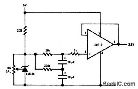
PRECISION_REFERENCE_LOW_NOISSE_BUFFERED_REFERENCE
Published:2009/7/1 2:37:00 Author:May
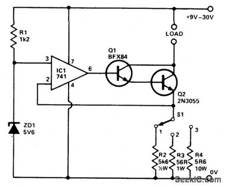
The circuit will provide 3 preset currents which will remain constant despite variations of ambient temperature or line voltage. ZD1 prifuces a temperature stable reference voltage which is applied to the noninverting input of IC1. 100% feedback is applied from the output to the inverting input holding the voltage at Q2s emitter at the same potential as the noninverting input. The current flowing into the load therefore is defined solely by the resistor selected by S1. Whic the values employed here, apreset current of 10 mA, 100 mA or 1 A van be selected. Q2 should be mounted on a suitabel heatsink. (View)
View full Circuit Diagram | Comments | Reading(705)
VOLTAGE_CONTROLLED_HIGH_SPEED_ONE_SHOT
Published:2009/7/1 2:36:00 Author:May
View full Circuit Diagram | Comments | Reading(690)
MEMORY_DRIVER_AMPLIFIER
Published:2009/7/24 4:08:00 Author:Jessie
Proves 750-ma current pulse for 8-mkrohenry load, at repetition role of 0.25 Mc. Positive turnoff voltage is automatically applied, with no extra loss in gain or power, by driving pnp transistor Q3 with npn transistor Q2.-J. S. Ronne, Computer Switching With High-Power Transistors, Electronics, 33:10, p 44-47. (View)
View full Circuit Diagram | Comments | Reading(696)
| Pages:1189/2234 At 2011811182118311841185118611871188118911901191119211931194119511961197119811991200Under 20 |
Circuit Categories
power supply circuit
Amplifier Circuit
Basic Circuit
LED and Light Circuit
Sensor Circuit
Signal Processing
Electrical Equipment Circuit
Control Circuit
Remote Control Circuit
A/D-D/A Converter Circuit
Audio Circuit
Measuring and Test Circuit
Communication Circuit
Computer-Related Circuit
555 Circuit
Automotive Circuit
Repairing Circuit