
Circuit Diagram
Index 1180
SINE_WAVE_DESCRAMBLER
Published:2009/7/1 5:16:00 Author:May
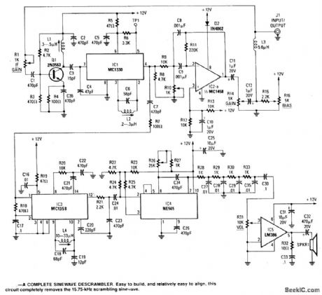
This decoder features a sine wave recovery channel and uses a PIN diode attenuator driven by the she wave recovery system to cancel out the she wave sync suppression signal. Kit available from North Country Radio, P.O. Box 53, Wykagyl Station, New York 10804. (View)
View full Circuit Diagram | Comments | Reading(2003)
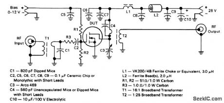
150_MHz_150_W_PEP_MOS_amplifier_28_V_supply
Published:2009/7/24 3:45:00 Author:Jessie
The electrical characteristics for the MRF140 shown in this circuit are given in Fig.2-52B. (View)
View full Circuit Diagram | Comments | Reading(648)
VERSATILE_MONO
Published:2009/7/1 5:15:00 Author:May
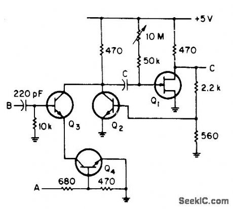
Uses standard digital IC voltage levels as inputs, and can be enabled or inhibited at any time without causing output pulse. Input gate Q3-Q4 is enabled with logic 1 at point A and inhibited with logic O.Logic 1 at B starts timing cycle. Q1 is 2N3819 JFET, and all other transistors are 2N3704.-R. Tenny, Versatile One-Shop, EEE Magazine, Sept. 1970, p 89 (View)
View full Circuit Diagram | Comments | Reading(683)
SAWTOOTH_VOLTAGE_GENERATOR_MODULATES_KLYSTRON
Published:2009/7/24 3:45:00 Author:Jessie
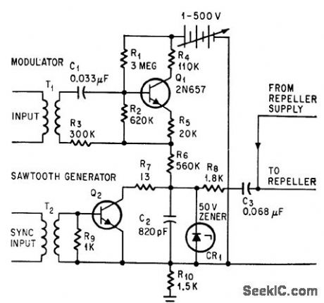
C2 is charged through R6 and discharged through Q2 operated in avalanche mode. Flyback time of sawtooth W.H. Chiles and H.G. Lafuse, Sweeping Carrier Signals Through Interference, Electronics, 37:16, p 94-96. (View)
View full Circuit Diagram | Comments | Reading(658)
FM_DEMODULATOR
Published:2009/7/1 5:14:00 Author:May
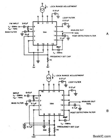
The NE564 is used as an FM demodulator. The connections for operation at 5 V and 12 V are shown in Figures 21-4A and 21-4B. The input signal is ac coupled with the output signal being extracted at Pin 14. Loop filtering is provided by the capacitors at Pins 4 and 5 with additional filtering being provided by the capacitor at Pin 14. Since the conversion gain of the VCO is not very high, to obtain sufftcient demodulated output signal the frequency deviation in the input signal should be 1% or higher. (View)
View full Circuit Diagram | Comments | Reading(0)
Strobed_strain_gauge_conditioner
Published:2009/7/24 3:44:00 Author:Jessie
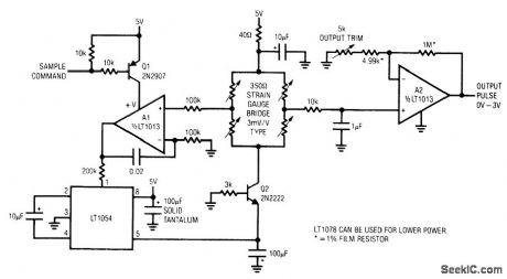
Fig. 14-14 This circuit also provides an output from a strain-gauge transducer on a sampled basis (to minimize power consumption), as does the circuit of Fig. 14-13. However, the Fig. 14-14 circuit is designed to remain in the quiescent state for long periods with relatively brief on-times, actuated by a sample or strobe command. A typical application would be for remote weight information in storage tanks, where weekly readings are sufficient. Quiescent current is about 150μA and on-state current about 50 mA. The output-trim pot scales the circuit for 3-mV/V-type strain-gauge transducers. Linear Technology Linear Applications Handbook 1990, p AN23-4. (View)
View full Circuit Diagram | Comments | Reading(1289)
AM_DEMODULATOR
Published:2009/7/1 5:12:00 Author:May
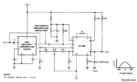
Amplifying and limiting of the AM carrier is accomplished by the if gain block providing 55 dB of gain or higher with a limiting of 40 μV. The limited carrier is then applied to the detector at the carrier ports to provide the desired switching function. The signal is then demodulated by the synchronous AM demodulator (1496) where the carrier frequency is attentuated due to the balanced nature of the device. Care must be taken not to overdrive the signal input so that distortion does not appear in the recorded audio.Maximum conversion gain is reached when the carrier signals are in phase as indicated by the phase-gain relationship. Output ftltering is also necessary to remove high frequency sum components of the carrier from the audio signal. (View)
View full Circuit Diagram | Comments | Reading(3300)
STEREO_DEMODULATOR
Published:2009/7/1 5:09:00 Author:May
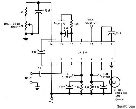
This circuit uses a single IC LM1310 to provide left and right outputs from a composite MPX stereo signal. Oscillator adjust R1 is set for 76 kHz (19 kHz at pin 10). C1 should be a silver mica or NPO ceramic capacitor. (View)
View full Circuit Diagram | Comments | Reading(1657)
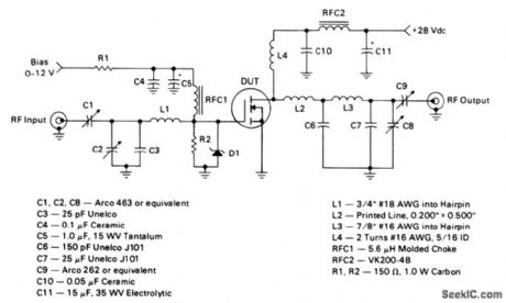
30_MHz_150_W_PEP_MOS_amplifier_28_V_supply
Published:2009/7/24 3:44:00 Author:Jessie
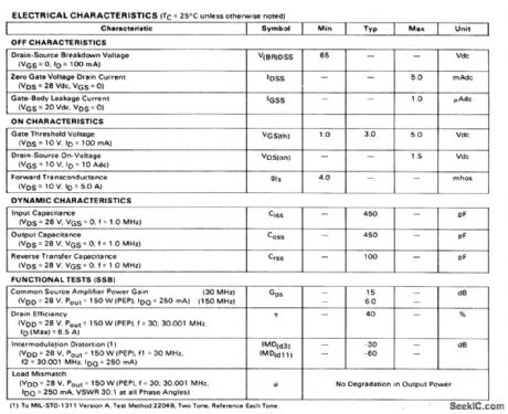
The electrical characteristics for the MRF140 shown in this circuit are given in Fig.2-52B (View)
View full Circuit Diagram | Comments | Reading(681)
TRANSISTORS_FOR_BC_221
Published:2009/7/1 5:07:00 Author:May
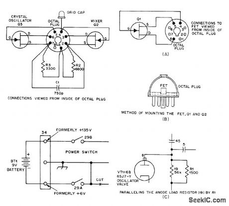
TRANSISTORS FOR BC-221-Old BC-221 frequency meter can be modernized by replacing its three now-scarce tubes with four 2N3819 Nchannel JFETs and changing supply to single 9 V battery. VT167 (6K8) mixer-oscillator is replaced by two JFETs with R2, R3, and 01 mounted inside octal plug. Resistance values may need some adjustment. Cut and insulate original leads to pins 2, 4, and 7, and connect top-cap clip of mixer tube to pin 4. VT116-B (6SJ7-Y) tube used for VFO is replaced by single 2N3819 connected as for Q1.Place 4K across 15K Add RI in parallel with plate load resistor; value depends on par-ticular FET used, and can range from 1 to 6800 ohms (1500 is typical). VT116 (6SJ7) beat-fre-quency amplifier is replaced by 2N3819 mounted same as for al. Place 4K across 15K load resistor of VT116-B and replace 300-ohm cathode resistor with one giving 1-mA source current (typically 1K to 3.3K). Total current drain is about 3 mA. Try 3-10 pF capacitor between gate and drain of 03 if circuit does not oscil-Iate.-R. S. N. Rau, Solid-State BC-221 Fre-quency Meter, 0ST, Feb. 1977, p 35-36. (View)
View full Circuit Diagram | Comments | Reading(3005)
SLOW_SWEEP
Published:2009/7/24 3:43:00 Author:Jessie
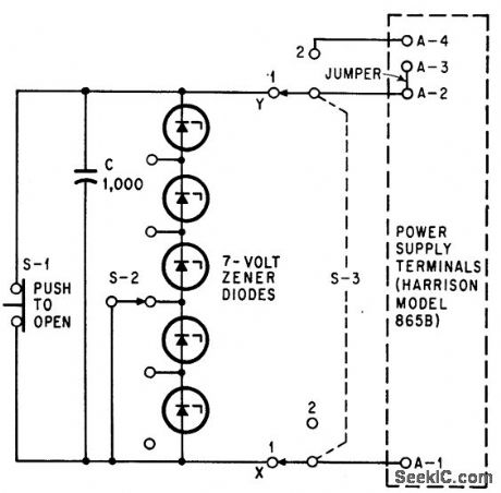
Large electrolytic capacitor and five zener diodes connected across standard transistor-regulated power supply give sweep voltage that increases 2 V per second, for classroom demonstrations.-M. H. Crothers, Added Capacitor Sweeps Power Supply, Electronics, 37:17, p 62. (View)
View full Circuit Diagram | Comments | Reading(632)
NARROW_BAND_FM_DEMODULATOR_WITH_CARRIER_DETECT
Published:2009/7/1 5:07:00 Author:May
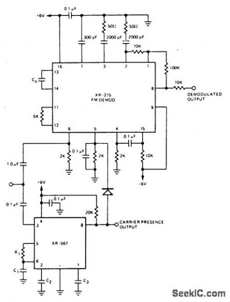
For FM demodulation applications where the bandwidth is less than 10% of the carrier frequency, an XR-567 can be used to detect the presence of the carrier signal. The output of the XR-567 is used to turn off the FM demodulator when no carrier is present, thus acting as a squelch. In the circuit shown, an XR-215 FM demodulator is used because of its wide dynamic range, high signal/noise ratio and low distortion.The XR-567 will detect the presence of a carrier at frequencies up to 500 kHz. (View)
View full Circuit Diagram | Comments | Reading(1321)
Improved_micropower_voltage_reference
Published:2009/7/24 3:43:00 Author:Jessie
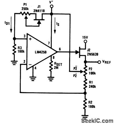
This circuit is an improved version of that shown in Fig. 8-44, but it requires an additional JFET to make the LM4250 independent of the unregulated input. (View)
View full Circuit Diagram | Comments | Reading(686)
TRIGGERED_BISTABLE
Published:2009/7/1 5:06:00 Author:May
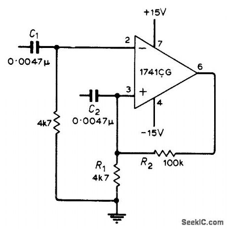
Positive feedback applied to opamp through R2 and R1 causes amplifier output to remain at either its positive or negative saturation limit. Triggering pulses for changing state of output may be applied to either input terminal, through C1 or C2; pulse polarity required to produce transition depends on state of circuit, which should be verified ex-perimentally.-G. B. Clayton, Experiments with Operational Amplifiers. Wireless World, May 1973. p 241-242. (View)
View full Circuit Diagram | Comments | Reading(775)
15_s_ASTABLE
Published:2009/7/1 5:01:00 Author:May
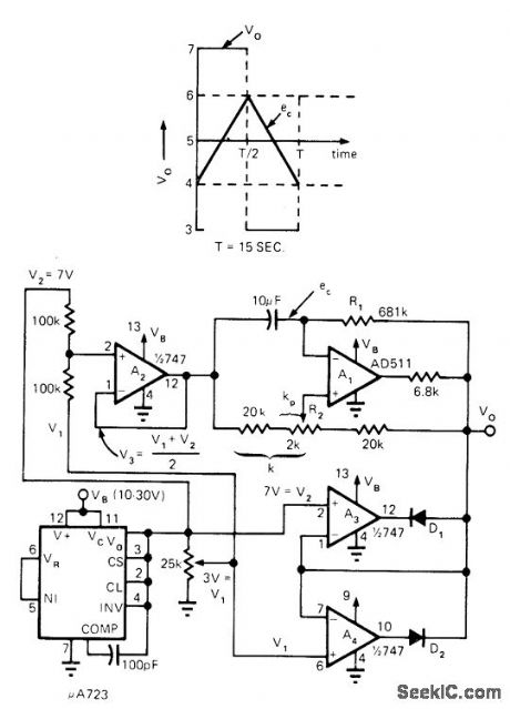
Precision opamp/diode clamp circuit simulating zener reduces cost of astable multivibrator having long time constant and good temperature stability. Circuit operates from single-ended supply, with μA723 providing 7-V referencefor clamp amplifiers A3 and A4. A2 provides oscillator with reference voltage V3 halfway between V1 and V2. R2 allows frequency of oscillator to be adjusted about ±6%. Article gives design equations.-L. Drake. Long Time-Constant Oscillator Uses Precision Clamps, EDN Magazine, Dec. 20, 1974, p 51-52. (View)
View full Circuit Diagram | Comments | Reading(792)
6_DIGIT_DRlVE
Published:2009/7/1 4:53:00 Author:May
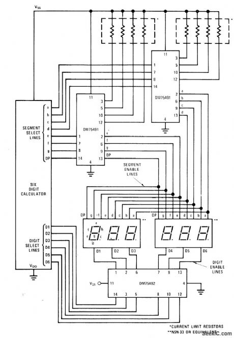
Uses two National DM75491 four-segment drivers for mutiltex-mocte display of MOS calculator. Total of eight segment drivers provides drivefor each one of seven segments plus logic control for decimal point.-C.Carinalli, Driving 7-Segment LED Displays with National Semiconductor Circuits, National Semiconductor, Santa Clara, CA, 1974, AN-99, p 9.
(View)
View full Circuit Diagram | Comments | Reading(1461)
REDUCING_LED_POWER_DRAIN
Published:2009/7/1 4:52:00 Author:May
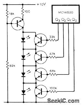
Arrangement of LEDs in groups of four with constant-current source greatly eliminates wastage of battery power Circuit shows utilization of this technique to display 4-bit binary number from CMOS counter.-T.R.Owen,L.E.D.Display,Wireless World,1976,P 72. (View)
View full Circuit Diagram | Comments | Reading(918)
VOLTAGE_CONTROLLED_MONO
Published:2009/7/1 4:52:00 Author:May
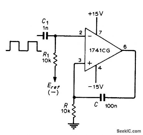
Timing period of opamp operating as monostable multivibrator is controlled by magnitude of DC reference voltage. With square-wave input shown. differentiating action by C1-R1 gives positive pulses that cause mono to make transitions. Article gives design equation and typical waveforms.-G. B. Clayton. Experiments with 0perational Amplifiers, Wireless World, May 1973, p241-242. (View)
View full Circuit Diagram | Comments | Reading(2921)
BAR_GRAPH_READOUT
Published:2009/7/1 4:50:00 Author:May
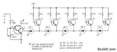
Transistors switch row of LEDs on in succession to give rising-bar display indicating input voltage. R2 can be ad-justed from minimum range of 0.1 to 0.5 V in 0.1-V increments for five LEDs to maxinlum of 1.0 to 10.0 V in 1-V increments. Input resistance of circuit is above 100,000 ohms.-F, M. Mims, Electronic Circuitbook 5: LED Projects, Howard W. Sams, Indianapolis, IN, 1976, p 86-88. (View)
View full Circuit Diagram | Comments | Reading(787)
OP_AMP_CLAMPING
Published:2009/7/1 4:49:00 Author:May
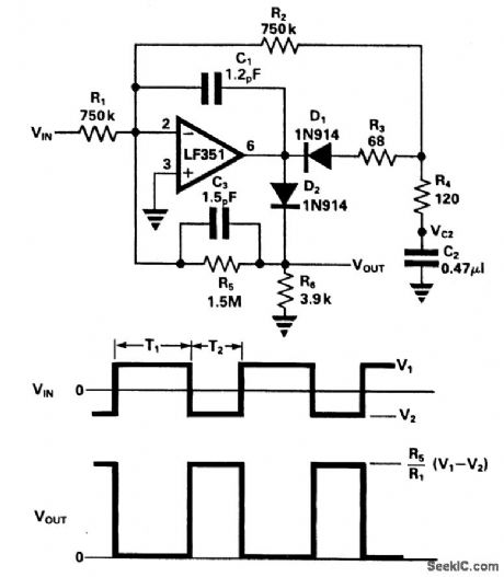
The circuit clamps the most positive value of the input pulse signal to the zero base level. Additionally, the circuit inverts and ampliftes the input signal by the factor of R5/R1. The waveforms are shown in the bottom of Fig. 2-24. (View)
View full Circuit Diagram | Comments | Reading(1210)
| Pages:1180/2234 At 2011611162116311641165116611671168116911701171117211731174117511761177117811791180Under 20 |
Circuit Categories
power supply circuit
Amplifier Circuit
Basic Circuit
LED and Light Circuit
Sensor Circuit
Signal Processing
Electrical Equipment Circuit
Control Circuit
Remote Control Circuit
A/D-D/A Converter Circuit
Audio Circuit
Measuring and Test Circuit
Communication Circuit
Computer-Related Circuit
555 Circuit
Automotive Circuit
Repairing Circuit