
Circuit Diagram
Index 1162
GIANT_NIXIE_SIGN
Published:2009/7/1 23:51:00 Author:May
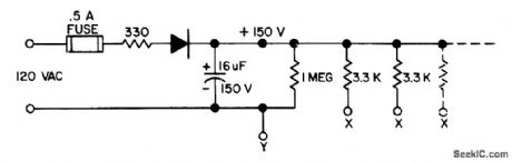
Simple power supply drives any desired number of alphameric Nixie characters each 21/2inches high to form illuminated house numbers, ON THE AIR sign for amateur station, or BAR IS CLOSED sign for party room. Connect 3.3K resistorfrom +150 V to pin 13 of each Nixie, and connect to point Y (-150 V) each segment to be lighted. Sign can be changed at any time by resoldering connections to segments.Diode must handle AC line voltage.-J.Grimes,Display Yourself in a Big Way,73 Magazine, Nov./Dec,1975,p 186-188. (View)
View full Circuit Diagram | Comments | Reading(631)
FIELD_STRENGTH_METER
Published:2009/7/1 23:51:00 Author:May
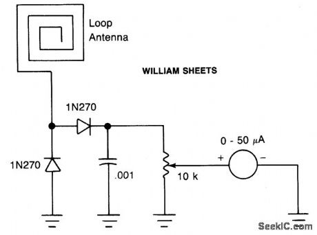
The antenna consists of about 20 cm of insulated stranded wire glued or taped around the inside of a small plastic box. RF current is rectified by two diodes, and a 10 k potentiometer provides variable attenuation for the meter. (View)
View full Circuit Diagram | Comments | Reading(0)
ORGAN_TONE_GENERATOR
Published:2009/7/1 23:50:00 Author:May
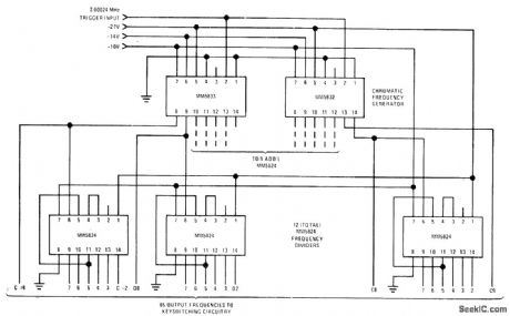
National MM5824 and MM5824 chromatic frequency generators are used with 12 MM5824 frequency dividers to generate 85 musical frequencies fully spanning equal-tempered octave. Can also be used as celeste or chorus tone generator and as electronic music synthesizer. Square-wave inputfor organ is 2.00024 MHz but can be as low as 7 kHz for other applications -''MOS/LSI Databook.'' national Semiconductor .Santa Clara. CA .1977.p3-11-3-13. (View)
View full Circuit Diagram | Comments | Reading(2262)
LED_DIMMER
Published:2009/7/1 23:49:00 Author:May
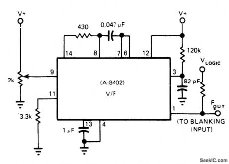
Intech/Function Modules A8402 is used in voltage-to-frequency mode to provide controllable dimming of LED display by varying frequency of blanking input to display driver. Display is pulsed on and off rapidly; the higher the duty cycle, the brighter the display.At highest input voltage the converter is forced out of linear region, making its mono remain on continuously for brightest display,-P. Pinter and D. Timm, Voltage-to-Frequency Converters-IC Versions Perform Accurate Data Conversion (and Much More) at Low Cost, EDN Magazine, Sept. 5, 1977, p 153-157. (View)
View full Circuit Diagram | Comments | Reading(872)
FIBEROPTIC_INTERFACE
Published:2009/7/1 23:47:00 Author:May
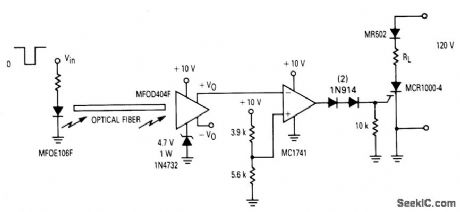
An op amp is used to interface between a fiberoptic system and the MOS SCR to multi-cycle,half-wave control of a load.This recelver has two complementary outputs,one at a quiescent level of about 0.6 V and the second at 3 V.By adding a 4.7 V zenerh senes with the return bus,the effective Vcc becomes 5.3V and also the 0.6V outputlevel is translated up to about 5.3 V.This level IS compatible with the reference input(5.9V) of the single-ended powered op-amp acting as a comparator. (View)
View full Circuit Diagram | Comments | Reading(772)
F_V_CONVERTER_
Published:2009/7/1 23:46:00 Author:May
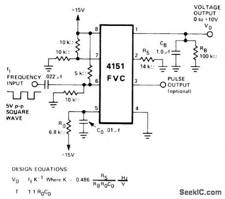
Single-suρply circuit uses frequency-to-voltage connection of RM4151converter to make output voltage vary between 0 and as frequency of 5 V P-P squarewave inρut varles bettween 0 and 10 kHz,-″Linear Integrated Circuit Data Book,'' RaytheonSemiconductor Division,Mountain View,CA, 1978,p 7-39. (View)
View full Circuit Diagram | Comments | Reading(1542)
DC_VARIABLE_SPEED_MOTOR_CONTROL_VIA_FIBEROPTICS
Published:2009/7/1 23:41:00 Author:May
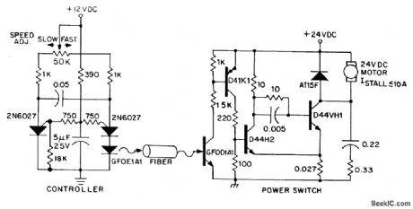
Dc power can also be controlled via fiberoptics. The circuit provides an insulated speed control path for a small dc actuator motor (≤1/12hp). Control logic is a selfcontained module requiring about 300 mW at 12 V, which can be battery powered. The control module furnishes infrared pulses, at a rate of 160 Hz, with a duty cycle deter-mined by the position of the speed adjust potentiometer. The programmable unijunction multivibrator provides approximately 10 mA pulses to the GFOE1A1 at duty cycles adjustable over a range of 1% to 99%. The infrared pulses are detected by the GFOD1A1, amplified by the D39C1 pnp Darlington, and supplied to the power drive switch, which is connected in a Schmitt trigger configuration to supply the motor voltage pulses during the infrared pulses. Thus, the motor's average supply voltage is pulse width modulated to the desired speed, while its current is maintained between pulses by the A115F free-wheeling diode. The snubber network connected in parallel with the power switch minimizes peak power dissipation in the output transistor, and enhancing reliability. Larger hp motors can be driven by adding another stage of current gain, while longer fiber range lengths can be obtained with an amplifier transistor driving the GFOE1A1. (View)
View full Circuit Diagram | Comments | Reading(1013)
10_MHz_FIBEROPTIC_RECEIVER
Published:2009/7/1 23:36:00 Author:May
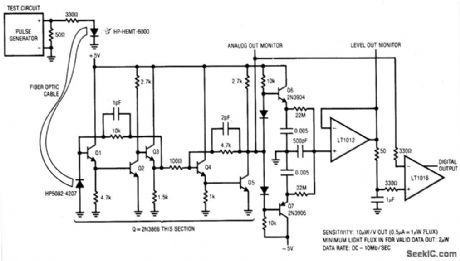
The receiver will accurately condition a wide range of light inputs at up to 10 MHz data rates.The optical signal is detected by the PIN photodiode and amplified by a broadband fed-back stage, Q1-Q3. A second, similar, stage gives further amplification.The output of this stage (Q5's collector) biases a 2-way peak detector (Q6-Q7). The maximum peak is stored in Q6's emitter capacitor while the minimum excursion is retained in Q7's emitter capacitor. The dc value of Q5's output signal's mid-point appears at the junction of the 0.005μF capacitor and the 22 M ohm unit. This point will always sit midway between the signal's excursions, regardless of absolute amplitude. This signal-adaptive voltage is buffered by the low bias LT1012 to set the trigger voltage at the LT1016's positive input. The LT1016's negative input is biased directly from Q5's collector. (View)
View full Circuit Diagram | Comments | Reading(1677)
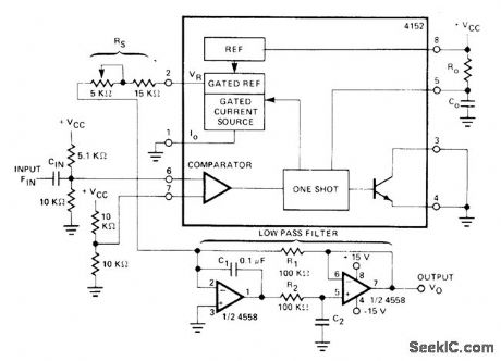
CCD_DELAY_FOR_SPECIAL_EFFECTS
Published:2009/7/1 23:32:00 Author:May
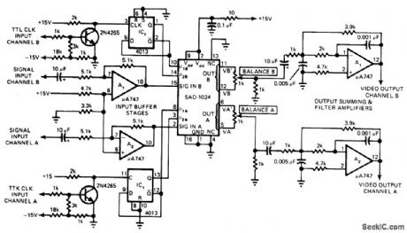
Basic bucket-brigade device incorporated in Reticon Corp. SAD-1024 charge-coupled-device delay line can synthesize such interesting audio-system delay effects as reverberation enhancement.chorus.and vibrato generation Other appIications include speech compression and voice scrambling Evaluation circuyt shown was developed by manulfacturer lnput clock frequencyis 200 kHz.and signal input is 5-kHz sine wave. Article describes operation of evaluation circuit in detail and presents variety of practical applications.-R. R. Buss. CCD's lmprove Audio System Performance and Generate Effects, EDN Magazine. Jan. 5. 1977. p55-61. (View)
View full Circuit Diagram | Comments | Reading(2724)
MOSFET_DIP_METER_
Published:2009/7/1 23:32:00 Author:May
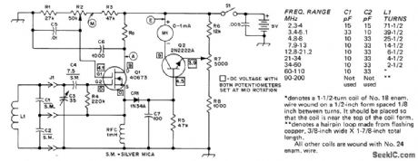
Output of groundeddrain Colpitts oscillator using RCA N-channel dual-gate MOSFETQ1 is detected by CR1 and amplified by Q2 for driving meter. Frequency of oscillation depends on C1, C2, C3, and L1, and reaches 250 MHz when L1 is reduced to hairpin.Table gives values of plug-in assembly L1-C1-C2 for nine frequency ranges. Circuit was designed for 12-V supply but works well with 9-V battery shown if drain resistor RD, is shorted. Battery drain is about 20 mA. All coils are wound on Millen 45004 forms.-F. Bruin, A Dual-Gate MOSFET Dip Meter, QST, Jan. 1977, p 16-17. (View)
View full Circuit Diagram | Comments | Reading(3029)
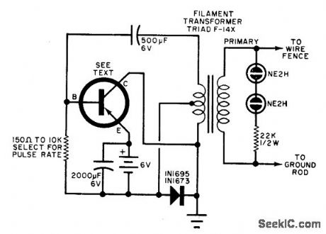
SOLID_STATE_ELECTRIC_FENCE_CHARGER
Published:2009/7/1 23:29:00 Author:May
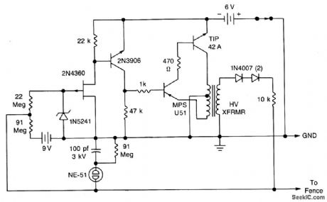
A touch-sensing circuit keeps the high-voltage generator cut off until something touches the fence wire. Contact with the fence sensing circuit wire starts the high-voltage generator which applies a series of 500 microsecond puises at approximately 300 volts to the fence wire. Pulse repetition rate is determined by the intruder's resistance to earth ground. The lower the resistance, the higher the pulse rate. A ground rod is inserted several inches into the ground near the fence wire. In the sensing mode the neon lamp should not flicker or light. If it does, it indicates leakage between the fence wire and ground. If sensitivity is too great, it can be reduced by changing the 91 Meg resistor to 47 or 22 Meg as required. (View)
View full Circuit Diagram | Comments | Reading(5495)
ELECTRIC_FENCE_CHARGER
Published:2009/7/1 23:25:00 Author:May
Any good power transistor can be used in this circuit. The base resistor should be adjusted to obtain a pulse rate of about 50 pulses per minute. The range of values shown can go from 10 pulses to 100 pulses per minute. The single fence wire must be insulated at each supporting pole and should be mounted low enough to prevent an animal from crawling under the wire.The two neon lamps indicate when the unit is operating. (View)
View full Circuit Diagram | Comments | Reading(11444)
5_×_7_DOT_MATRIX
Published:2009/7/1 23:25:00 Author:May
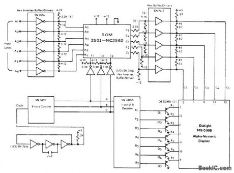
Drive for Dialight 745-0005 64-character alphamerle display generates desired character in response to pattern of 0s and 1s on input lines A1-A6. Timing of sequential scanning operation for seven horizontal rows of matrix is controlled by clock that drives binary counter having row-selecting outputs A, B, and C. Outputs C1-C5 of ROM correspond to vertical rows of dots enabled by 1-out-of-8 decoder.- Readout Displays, Dialight,Brooklyn, NY,1978,Catalog SG745,p 24-26. (View)
View full Circuit Diagram | Comments | Reading(994)
BATTERY_POWERED_FENCE_CHARGER
Published:2009/7/1 23:22:00 Author:May

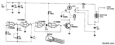

In essence, the circuit is nothing more than an auto ignition coil and a set of points which accomplishes the same thing. A pulsing circuit made from a single CMOS NOR integrated circuit (U1), opens and closes the relay contacts to simulate the action of the original breaker points. The relay pulser is divided into two clocking functions. The first circuit is a free-running squarewave generator that determines the rate or frequency of the pulses that activate the relay. It is essentially a pair of NOR gates connected as inverters and placed in a feedback loop, they are U1-b. The oscillating period of the feedback loop is determined by timing components C1, R1, and variable resistor R5. (View)
View full Circuit Diagram | Comments | Reading(1607)
VOLTAGE_CONTROLLED_FILTER
Published:2009/7/1 23:22:00 Author:May
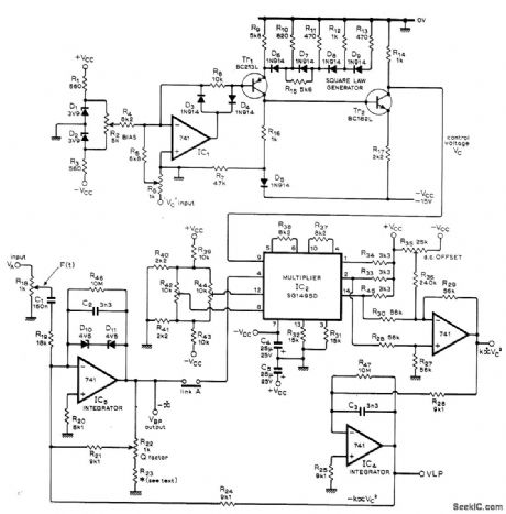
Used in elaborate sound synthesizer developed for generating wide variety of sounds. Serves as bandpass filter for which resonant frequency is Iinearly proportional to sum of input control voltages and a bias voltage. Can also be used as notch filter or as spectrum analyzer. Three-part articledescribes operation in detail and gives all other circuits of synthesizer. Supply voltages are 15 V.with polarity as indicated.-T. 0rr and D W. Thomas. Electronic sound Synthesizer、Wireless World. Part 2--Sept 1973.p 429-434(Part 1-Aug 1973.p366-372; Part 3-Oct.1973.p 485-490) (View)
View full Circuit Diagram | Comments | Reading(3341)
POSITIVE_INPUT_GIVES_RED
Published:2009/7/1 23:21:00 Author:May
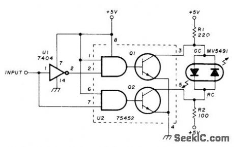
Uses Monsanto MV5491 dual LED having red and green light emitting diodes connected inversely in parallel,so current in onedirection gives green light and reverse current gives red. Circuit uses single SN75452 IC driver and one section of SN7404 hex inverter. High or positive input gives red indication, while low input gives green. Current limiting resistors R1 and R2 have different values because voltage and current specifications of parallel LEDs are different. Indicator appears to change color as input changes.-K. Powell,Novel Indicator Circuit, Ham Radio, April 1977,p 60-63. (View)
View full Circuit Diagram | Comments | Reading(1684)
OPAMP_DRIVESLED
Published:2009/7/1 23:19:00 Author:May
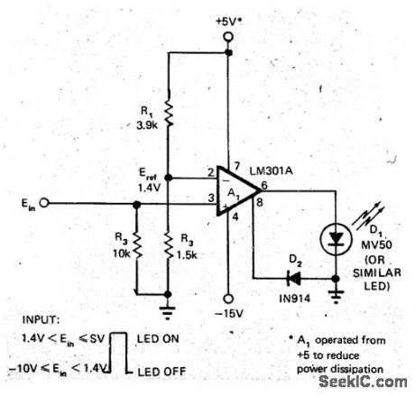
LM301A is used as open-Ioop voltage comparator, with LED receiving total source current of about 20 mA from opamp. Input is TTL-compatible, with R1-R2 reference divider biasing opamp in center of TTL output transition region. Circuit realizes full open-loop speed of opamp since it is uncompensated and its internal voltage amplifier stages are kept out of saturation by clamping of D2 and by inherent current-limiting action. Response times for toggling LED are in microsecond range.-W. G. Jung, Poor Man's LED Driver is TTL Compatible, EDN Magazine, Feb.5, 1973, p 86. (View)
View full Circuit Diagram | Comments | Reading(1322)
10O_LED_SOLID_STATE_OSClLLOSCOPE
Published:2009/7/1 23:18:00 Author:May
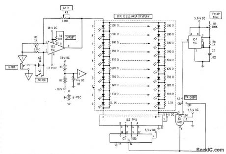
Flat display of LEDs replaces cathode-ray tube of oscilloscope. Suitable for classroom demonstrations even though resolution is poor. Amplified input signal is fed to upper ends of all ten vertical columns of LEDs. Under control of time base, scanner completes circuit at bottom of each column in turn. Vertical columns are made voltage-sensitive by resistors paralleling LEDs.Gate circuit using section of 7400 provides triggering when desired. Vohage-sensitive bargraph readouts formed by vertical columns are scanned by 7490 decade counter and 7441 decoder. Sweep rate of display is adjustable from 1 to 20 vertical columns per second with R5.-F,M Mims, Electronic Circuitbook 5: LED Projects, Howard Sams,Indianaplis,IN,1976,p 92-96. (View)
View full Circuit Diagram | Comments | Reading(2994)
JFET_ac_COUPLED_INTEGRATOR
Published:2009/7/1 23:16:00 Author:May
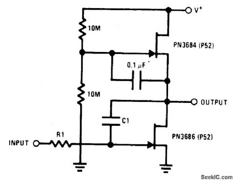
This circuit utilizes the μ-amp technique to achieve very high voltage gain. Using C1 in the circuit as a Miller integrator, or capacitance multiplier, allows this simple circuit to handle very long time constants. (View)
View full Circuit Diagram | Comments | Reading(1292)
31_2_DIGIT_MULTIPLEXED_LCD
Published:2009/7/1 23:15:00 Author:May
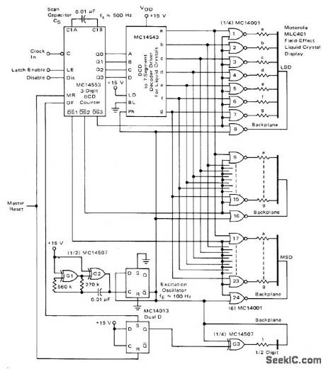
Uses MLC401 field-effect liquid crystal display, which is more suitable for multiplexing than dynamic-scattering LCD. Counters, latches, multiplexet, and scan circuits are all inMC14553 3-digit BCD counter whose outputs feed MC14543 decoder and driver for display. Excitation frequency of 100 Hz is derived from square-wave oscillator G1-G2 having exactly 50% duty cycle. Scan frequency is about 500 Hz, giving display refresh rate of 170 Hz, which is well beyond detectable flicker rate.-A. Pshaenich, Interface Considerations for Numeric Display Systems, Motorola, Phoenix, AZ, 1975, AN-741, p 6. (View)
View full Circuit Diagram | Comments | Reading(1550)
| Pages:1162/2234 At 2011611162116311641165116611671168116911701171117211731174117511761177117811791180Under 20 |
Circuit Categories
power supply circuit
Amplifier Circuit
Basic Circuit
LED and Light Circuit
Sensor Circuit
Signal Processing
Electrical Equipment Circuit
Control Circuit
Remote Control Circuit
A/D-D/A Converter Circuit
Audio Circuit
Measuring and Test Circuit
Communication Circuit
Computer-Related Circuit
555 Circuit
Automotive Circuit
Repairing Circuit