
Circuit Diagram
Index 1193
Zero_crossing_detector_for_squaring_a_sine_wave
Published:2009/7/24 4:31:00 Author:Jessie
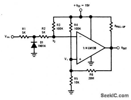
Fig. 15-15 This circuit symmetrically squares a sine wave (centered around 0 V) by introducing a small amount of positive feedback. Using the values shown, V1= V2 when VIN is zero. D1 ensures that the inverting input never goes below -100 mV and V2 never goes below ground. National Semiconductor Linear Applications Handbook 1991, p. 260. (View)
View full Circuit Diagram | Comments | Reading(1091)
DIRECT_REPRODUCE_CIRCUIT
Published:2009/7/24 4:31:00 Author:Jessie
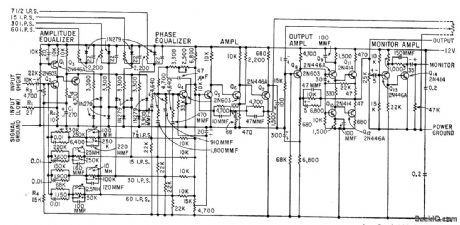
Switching and equalization networks extend upper frequency limit to 250 kc for instrumentation tape. Amplifier section provides voltage gain of 14 db and output impedance below 50 ohms, for driving long, low-impedance lines.-D. R, Steele, More Bandwidth for Magnetic Recorders, Electronics, 33:2, p 44-47. (View)
View full Circuit Diagram | Comments | Reading(772)
Charge_pump_LCD_contrast_supply
Published:2009/7/24 5:30:00 Author:Jessie
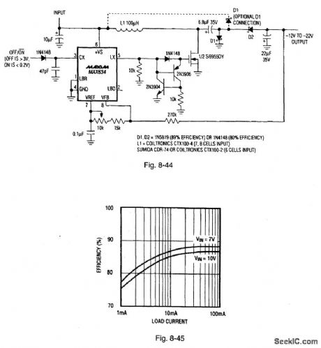
Figure 8-44 shows a MAX634 connected as an LCD-contrast supply using the charge-pump principle for higher efficiency. Figure 8-45 shows the efficiency curves. This circuit is particularly useful where the LCD supply must be operated directly from the battery. (The circuit is a hybrid in that the switching regulator boosts the input to a high positive output voltage, with the actual negative output voltage being generated by a charge-pump tap on the switching node.) The circuit operates over a 4-V to 16-V (four-to eight-cell) range, draws 330 μA of quiescent current, and is capable of a 30-mA output. The optional D1 connection (dotted line) is used when the battery voltage exceeds the absolute value of the output voltage. If this does not occur, connect D1 to ground. MAXIM BATTERY MANAGEMENT CIRCUIT COLLECTION, 1994, P. 49, 50.
(View)
View full Circuit Diagram | Comments | Reading(731)
Ac_driven_bridge_synchronous_demodulator
Published:2009/7/24 5:29:00 Author:Jessie
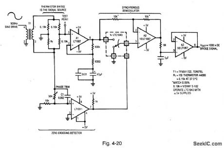
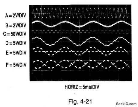
Figure 4-20 shows a circuit that combines a bridge with a synchronous detector to obtain very high noise rejection capability. Figure 4-21 shows the waveforms. Traces A, B, C, D, E, and F show T1 input, A1 input, LTC1043 clock, A1 output, A2 positive input, and A2 output, respectively. An ac carrier excites the bridge and synchronizes the gain-stage demodulator. In this application, the signal source is a thermistor bridge that detects extremely small temperature shifts in a biochemical microcalorimetry-reaction chamber. To calibrate, adjust the phase pot so that C1 switches when the carrier crosses through zero. LINEAR TECHNOLOGY, APPLICATION NOTE 43, P. 24. (View)
View full Circuit Diagram | Comments | Reading(2005)
Low_voltage_power_disconnect
Published:2009/7/24 5:29:00 Author:Jessie
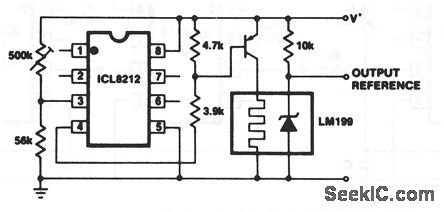
This circuit removes the power supply if the supply voltage drops below a certain value. As an example, the National Semiconductor LM199 precision reference has an on-chip heater that malfunctions with supply voltages below 9 V and it causes excessive device temperature. Using the values shown, the ICL8212 detects a supply voltage of 9 (or less) and turns off the supply to the LM199. (View)
View full Circuit Diagram | Comments | Reading(973)
Microporter_LCD_contrast_supply
Published:2009/7/24 5:28:00 Author:Jessie
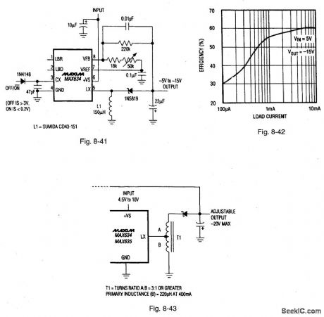
Figure 8-41 shows a MAX634 connected as a micropower LCD-contrast supply with an adjustable -5-V to -15-V output. Figure 8-42 shows the efficiency curve. This flea-power circuit is suitable for small multiplexed LCD displays (such as those on cellular phones). The circuit operates over a 4-V to 6-V range (with a maximum input/output differential of 24 V), draws 500-μA quiescent current, and is capable of 10-μA output. Figure 8-43 shows a way to extend the maximum input/output of 24-V by substituting an autotransformer for the inductor. MAXIM BATTERY MANAGEMENT CIRCUIT COLLECTION, 1994, P. 48.
(View)
View full Circuit Diagram | Comments | Reading(683)
Dc_dc_converter
Published:2009/7/24 5:28:00 Author:Jessie
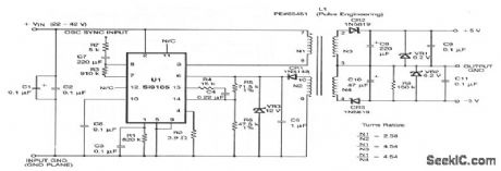
Although this circuit is designed to meet CCITT Standard 1.430 for ISDN (Integrated Services Digital Network) terminals, the circuit can be used for any battery-operated 15-V power-supply application. The input voltage is 22 to 42 V for maximum loads, and 30 to 42 V for minimum loads. Typical minimum loads are 3 mA at +5 V, and 0 mA at -5 V. Typical maximum loads are 100 mA at +5 V and 30 mA at -5 V. Ripple is 100 mV maximum at full load, and 60 mV typical at full load. Regulation is±5% typical and±7% worstcase. (View)
View full Circuit Diagram | Comments | Reading(0)
Nonvolatile_power_supply_malfunction_detector
Published:2009/7/24 5:19:00 Author:Jessie
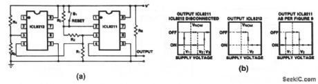
This circuit detects and stores the fact that an out-of-operating-range supply-voltage condition has occurred-even when the supply drops to 0. The circuit works on both high and low supply malfunctions so that the circuit can detect when a low supply voltage might have caused a volatile memory loss, or when an overvoltage might have damaged components, or any similar transient/intermittent power failure. The circuit operates with any supply range between 2 and 30 V. Figure 9-23B shows the output states as a function of supply voltage.Figure 9-21B shows the equations to calculate resistor values. The ICL8212 detects voltage V2, which is the upper limit of the operating voltage range. The ICL8211 detects the lower voltage limit of range V1. Hysteresis is used with the ICL8211 so that the output can be stable in either state over the operating voltage range from V1 to V2 by making V3 (the upper trip point of the ICL8211) much higher in voltage than V2. The ICL8212 output forces the ICL8211 output into the on-state above V2 Thus, there is no value of supply voltage that will result in the output of ICL8211 charging from the on-state to the off-state. This can be achieved only by shorting out R3 for values of supply voltage between V1 and V2. (View)
View full Circuit Diagram | Comments | Reading(780)
Universal_input_power_supply
Published:2009/7/24 5:19:00 Author:Jessie
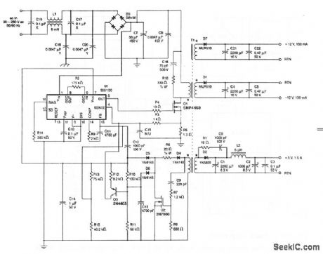
This circuit operates directly from 100-, 110-, and 220-V without the use of selector switches or jumpers (permitting the supply to be plugged into wall outlets anywhere in the world). T1 is a Schott Corp. #67122700, L1 is a Renco 1361- 2 common-mode choke, L2 is any 6-μH 1.5-A inductor, and D3 is a 1-A 600-V bridge. (View)
View full Circuit Diagram | Comments | Reading(2527)
Fast_charger_with_linear_regulator_current_source
Published:2009/7/24 5:19:00 Author:Jessie
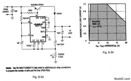
Figure 8-33 shows the MAX713 connected to provide a fast charge (with linear regulation) to both NiCad and NiMH batteries. This circuit solves two closely related problems found in portable power supplies. The circuit charges the battery and switches over from battery power to ac power when an external ac/dc adapter is plugged in. The MAX713 supplies the system load current (while the battery is being charged) by sensing and dynamically regulating the battery current. Figure 8-34 shows the operating area of the circuit. The MAX713 must be programmed for the desired number of cells; charging time, using pin straps, is described in the data sheet. MAXIM BATTERY MANAGEMENT CIRCUIT COLLECTION, 1994, P. 2.
(View)
View full Circuit Diagram | Comments | Reading(1195)
Low_power_bridge
Published:2009/7/24 5:18:00 Author:Jessie
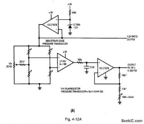
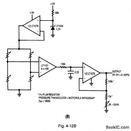
Figure 4-12A is identical to Fig. 4-1, except that the bridge excitation is reduced to 1.2V. This cuts bridge current from about 30 mA to about 3.5 mA. A 0.01% reading of a 10-V powered 350-Ω strain-gauge bridge (Fig. 4-1) requires 3 μV of stable resolution. The Fig. 4-12A circuit requires only 360 nV. Figure 4-12B is similar, but the bridge current is reduced below 700 μA. LINEAR TECHNOLOGY, APPLICATION NOTE 43, P. 18. (View)
View full Circuit Diagram | Comments | Reading(942)
Linear_output_thermistor_bridge
Published:2009/7/24 5:17:00 Author:Jessie

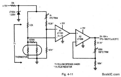

Figure 4-11 uses a thermistor in one leg of the bridge circuit. A trim in the opposing leg sets the bridge output to zero at 0℃. A1 and A2 provide additional trimmed gain to furnish a calibrated output. Calibration is performed in similar fashion to the platinum RTD circuits (Figs. 4-9 and 4-10). LINEAR TECHNOLOGY, APPLICATION NOTE 43, P. 17. (View)
View full Circuit Diagram | Comments | Reading(1342)
Precision_current_sink_source
Published:2009/7/24 5:16:00 Author:Jessie
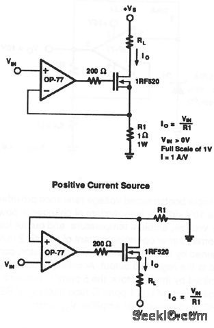
These circuits provide positive current-sink and current-source capability. (View)
View full Circuit Diagram | Comments | Reading(3097)
Linearized_platinum_RTD_resistance_bridge_switched_capacitor
Published:2009/7/24 5:15:00 Author:Jessie
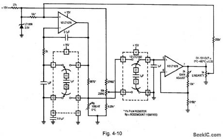
Figure 4-10 is a switched-capacitor version of the Fig. 4-9 circuit, with A2 and A3 replaced with an LTC1043. The differential-to-single-ended transitions in the current-source and bridge-output amplifier are performed by the LTC1043. The values shifts in the current source and output stage reflect the LTC1043 lack of gain. The primary trade-off between the two circuits is component count versus cost. LINEAR TECHNOLOGY, APPLICATION NOTE 43, P. 12. (View)
View full Circuit Diagram | Comments | Reading(990)
FM_remote_speaker_system
Published:2009/7/24 4:41:00 Author:Jessie

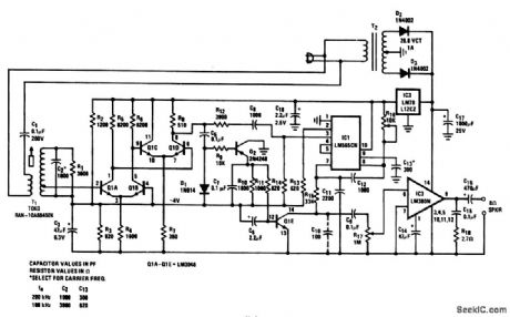
This complete carrier system is suitable for(high-qualit transmission of speech or music, and will operate from any ac outlet anywhere on a one-acre homesite. The frequency response is 20 to 20,000 Hz and THD_is under 0.5% for speech and music program material. The transmitter (Fig. 2-62A and 2-62C) is plugged into the ac line at a radio or stereo-system source The signal for the transmitter is ideally taken from the Monitor or Tape out connectors provided on component-system hi-fi receivers. The receiver (Fig 2-62B and 2:62B) amplifier ,limits, and demodulates the received FM signal in the presence of line-transient interference (sometimes as high as several hundred volts peak). The receiver also provides audio-mute in the absence of a carrier and 2.5-W audio output to a speaker. Transmitter carrier frequency fc is fixed near 100 or 200 kHz by C4/C7.The exact frequency is not important because T1 for both transmitter and receiver are tuned for maximum coupling to and from the ac line. Of course, both receiver and transmitter must be at the same frequency. With both transmitter and receiver operating (modulation is not necessary), tune the transmitter T1 for maximum, as measured with an ac VTVM at the receiver T1 secondary. Then tune the receiver T1 for maximum. Repeat as necessary. Set the receiver PLL free-running frequency with R16 near the center of its range. Rotate slowly in either direction until the PLL loses lock (as shown by a sharp increase in noise and a distorted output). Note the position of R16, and then repeat, rotating in the other direction. Note the new position, then center R16 between the two noted positions (a fine adjustment can be made for minimum noise if there is an SCR dimmer used in the house). Connect an audio signal to the transmitter input, and adjust RI for a maximum signal of about 0.1 V rms at pin 5 of IC1. This completes the adjustment. However, it might be necessary to readjust the receiver T1 slightly to minimize noise from SCR dimmers. (View)
View full Circuit Diagram | Comments | Reading(1285)
Comparing_voltages_of_opposite_polarity
Published:2009/7/24 4:40:00 Author:Jessie
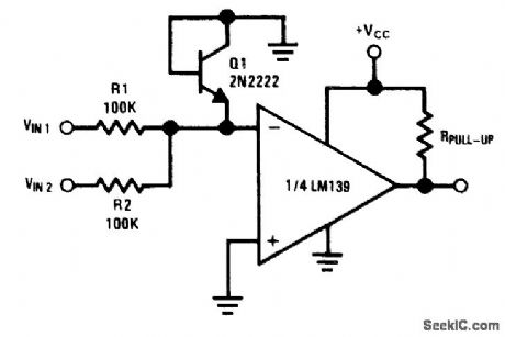
Fig. 15-22 This circuit compares the magnitude of VIN1 and VIN2, which have opposite polarities. The voltage at the inverting input of the LM139 is a function of VIN1, VIN2, R1, and R2. Diode-connected Q1 clamps the inverting terminal below ground for protection. If VIN1 is used for positive and VIN2 for negative, the output goes low (ground) if VIN1 is greater than VIN2. The output goes to near VCC if VIN1 is less than VIN2 National Semiconductor. Linear Applications Handbook, 1991, p. 260. (View)
View full Circuit Diagram | Comments | Reading(842)
Extendmg_line_opemted_three_termmal_regulrztor_caypability
Published:2009/7/24 4:39:00 Author:Jessie
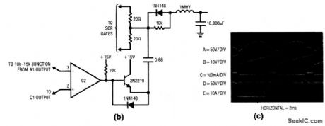
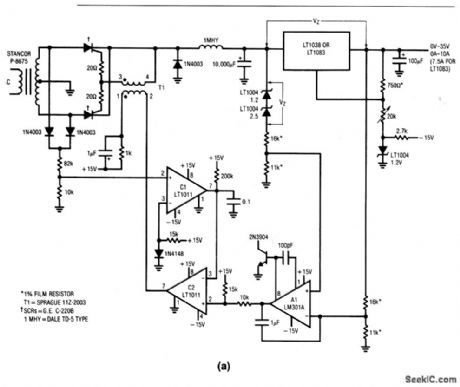
This ac-powered circuit provides 0- to 35-V, 10-A regulation under high-low (90 to 140 Vac) conditions. The transformer output is diode rectified (trace A, Fig. 9-10C), divided down, and used to reset the 0.1-μF capacitor (trace B) via C1. The resulting ramp at C1 is compared to the A1 output by C2. When the ramp exceeds the C2 noninverting input value, C2 goes low and dumps current through the T1 primary (trace C). This fires the appropriate SCR and creates a path from the main transformer to the LC filter (trace D). The resultant current flow (trace E) is limited by the inductor and charges the capacitor. When the ac line cycle drops low enough, the SCR commutates and charging ceases. Figure 9-10B shows a way to trigger the SCRs without a transformer. (View)
View full Circuit Diagram | Comments | Reading(805)
Noninverting_voltage_gain_stage_with_15_V_output
Published:2009/7/24 4:38:00 Author:Jessie
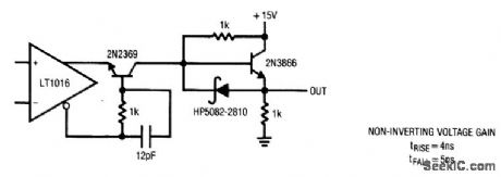
Fig. 15-21 This circuit uses a high-speed comparator (LT1016) and two transistors to provide a fast voltage-gain stage. When the LT1016 switches, the base-emitter voltages at the 2N2369 reverse and cause the transistor to switch rapidly. The 2N3866 emitter follower produces a low-impedance output and the Schottky diode aids current-sink capability, Linear Technology, Linear Applications Handbook 1990, AN13-31. (View)
View full Circuit Diagram | Comments | Reading(721)
Fully_isolated_limit_comparator
Published:2009/7/24 4:36:00 Author:Jessie
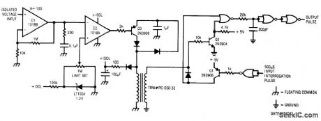
Fig. 15-20 This circuit produces a digital output if the input is above or below a preset limit, and is ideal for process-control applications where transducers operate at high common-mode voltage, or where large loops exist. Amplifier C1 permits use of thermocouples and other low-level sources. The circuit functions by echoing an interrogation pulse if the input is above a preset level. If the input is below the leve1 (determined by the 1-MΩ level set), no echo occurs. Maximum common-mode voltage is limited by the transformers 500-V breakdown. Linear Technology, Linear Applications Handbook 1990, p. AN11-10. (View)
View full Circuit Diagram | Comments | Reading(589)
F_M_DEMODULATOR_FOR_TAPE_RECORDER
Published:2009/7/24 4:36:00 Author:Jessie
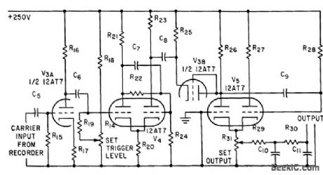
Removes low-frequency frequency-modulated nerve-potential signal from 7.5-kc carrier recorded on magnetic tope. Amplifier V3a feeds squarer V4 that is connected as Schmitt trigger to give square-wave output for differentiation by C8-R25. Negative going edge , of resulting square wave triggers monostable mvbr V5 which serves as demodulator.-K. D. Broadfoot, F-M Magnetic Tape System Records Low-Frequency Nerve-Fiber Potentials, Electronics, 34;28, p 66-67. (View)
View full Circuit Diagram | Comments | Reading(791)
| Pages:1193/2234 At 2011811182118311841185118611871188118911901191119211931194119511961197119811991200Under 20 |
Circuit Categories
power supply circuit
Amplifier Circuit
Basic Circuit
LED and Light Circuit
Sensor Circuit
Signal Processing
Electrical Equipment Circuit
Control Circuit
Remote Control Circuit
A/D-D/A Converter Circuit
Audio Circuit
Measuring and Test Circuit
Communication Circuit
Computer-Related Circuit
555 Circuit
Automotive Circuit
Repairing Circuit