
Circuit Diagram
Index 1192
15_V_RECEIVER_POWER_SUPPLY_CHARGER
Published:2009/7/24 4:30:00 Author:Jessie
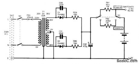
This power supply is for powering a receiver or similar load at 15 V, 100 mA. The NiCd battery pack is a 600-mAh AA cell assembly and is charged at 50 to 60 rnA. A 120-V primary transformer with the same secondary voltage can be substituted for the 230-V unit shown. (View)
View full Circuit Diagram | Comments | Reading(724)
Limit_comparator_with_lamp_driver
Published:2009/7/24 4:30:00 Author:Jessie
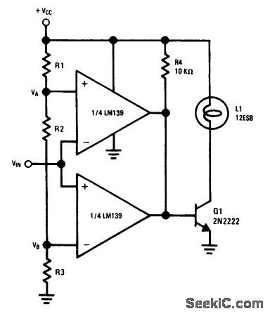
Fig. 15-14 This circuit provides a range of input voltages between which the outputs of both LM139 comparators will be off, allowing Q1 base current to flow through R4. This turns Q1 on and applies power to L1. If VIN changes to a value greater than VA, but less than VB, one LM139 switches on, shorting the Q1 base to ground. This turns lamp L1 off. If a pnp is used for Q1 (with emitter tied to + VCC), L1 will turn on when the input is above VA or below VB. The values of R1,R2, and R3 set the VA and VB points. For example, if VCC is 12 V, and all three resistors are the same value, VB is 4V, and VA is 8 V. National Semiconductor Linear Applications Handbook 1991, p. 260. (View)
View full Circuit Diagram | Comments | Reading(939)
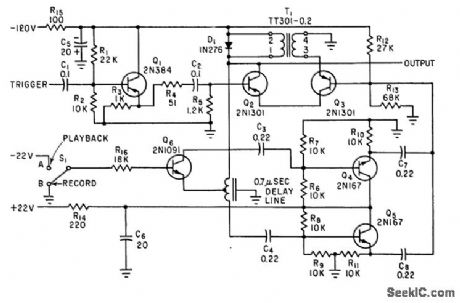
SYNCHRONOUS_DETECTOR_FOR_ZERO_SPEED_TAPE_PLAYBACK
Published:2009/7/24 4:30:00 Author:Jessie
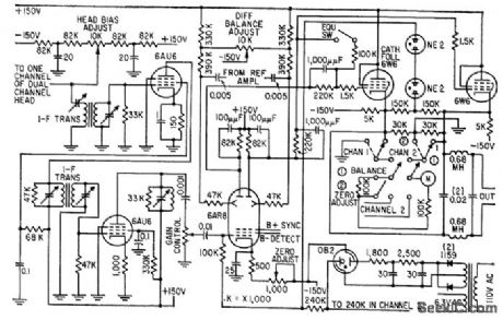
Tuned amplifiers with 200-kc center frequency and 20.kc bandwidth separate second harmonic signal containing intelligence from composite head output signal. Output of 6AR8 coupled to push-pull stage gives balanced output.-M. E. Anderson, Magnetic Head Reads Tape at Zero Speed, Electronics, 32:10, p 58-60. (View)
View full Circuit Diagram | Comments | Reading(1023)
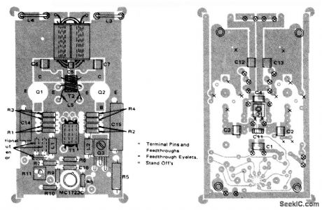
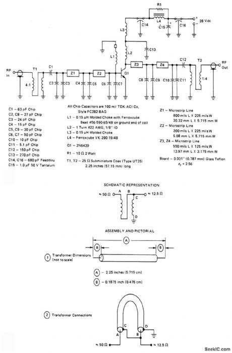
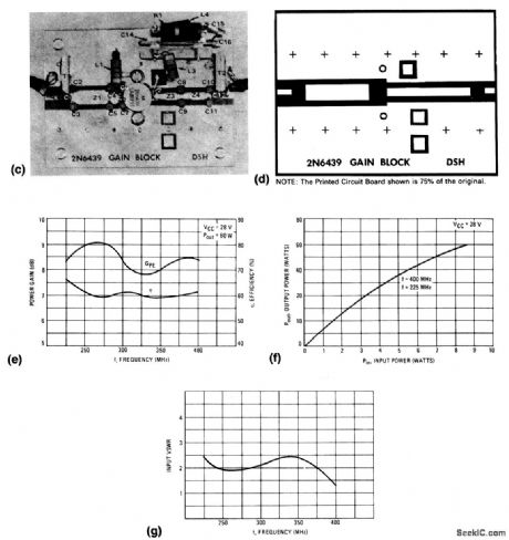
225_to_400_MHz_10_W_amplifier_28_V_supply
Published:2009/7/24 4:29:00 Author:Jessie
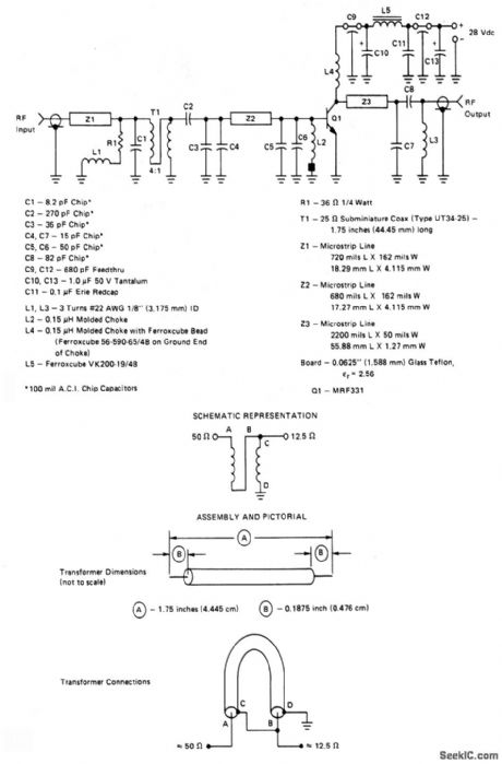
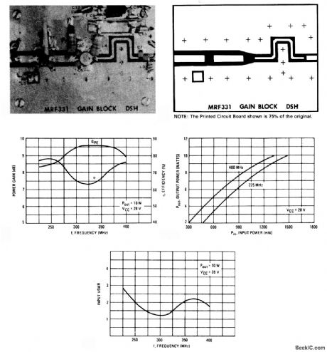
This amplifier can be used as is, or as a driver for higher-power devices. Figure 2-58B shows the construction details for transformer T1. Figures 2-58C and 2-58D show the component layout, and PC-board layout, respectively.Figures 2-58E, 2-58F, and 2-58G show typical amplifier performance characteristics. Those not familiar with microstrip techniques (for Z1, Z2, and Z3) should read the many Motorola publications, such as AN548A and AN555. (View)
View full Circuit Diagram | Comments | Reading(676)
HIGH_CURRENT_POWER_SUPPLY
Published:2009/7/24 4:29:00 Author:Jessie
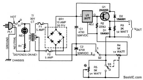
This 10-A power supply uses a 24- to 30-V center-tapped power transformer that is capable of delivering 5 to 10 A. The voltage output is controlled by the circuit consisting of R4, R5, and S3; note that S3 is part of R4. For a fixed-voltage output, R4 should be set for zero ohms (fully counterclockwise). In that position, switch 53, will open. Trimmer potentiometer R5 should then be adjusted so that the circuit produces a 12-V output (or whatever output your application demands). For an adjustable output, R4 is turned clockwise, closing S3, and removing R5 from the circuit. The output voltage is then controlled by the resistance offered by R4 alone. When SPDT switch S2 is in position 1, the maximum output current is achieved, with both halves of T1 providing current to the filter section to double the overall current output. However, the maximum output voltage is halved in that position. That is a more efficient setting because the power transistor need not drop as large a voltage. In position 2, the maximum voltage almost equals the rating of T1. D1 and D2 are included in case power is turned off with an inductive load attached. (View)
View full Circuit Diagram | Comments | Reading(1819)
MEMORY_MATRIX_SWITCHING
Published:2009/7/24 4:28:00 Author:Jessie
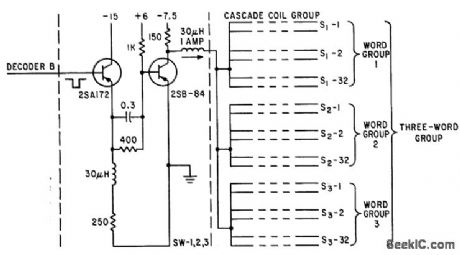
Output terminal, connected to throe word coil groups of matrix, is grounded when pulse appears at input.-J. Yamato and Y. Suzuki, Forming Semi-Permanent Memories with Metal Cord Storage, Electronics, 34:46, p 136-141. (View)
View full Circuit Diagram | Comments | Reading(678)
A_C_RELAY_DRIVE
Published:2009/7/24 4:28:00 Author:Jessie
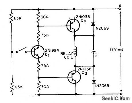
Drives 12-V ac relay with transistors triggered by low direct current of pair of switch contacts. Can drive any a-c relay rated in voltage up to breakdown rating of transistors.-R. K. Walters, Transistor Driven AC Relay, EEE, 11:2, p 25-26. (View)
View full Circuit Diagram | Comments | Reading(1263)
2_to_30_MHz_300_W_PEP_linear_amplifier_28_V_suplly
Published:2009/7/24 4:27:00 Author:Jessie

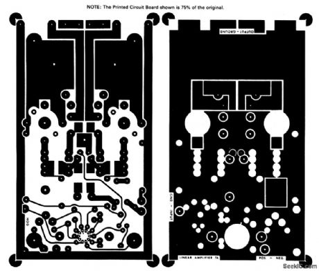
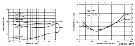
This push-pull linear amplifier provides 300-W of PEP Or CW output power across the 2-to 30-MHz band. The component layout, and PC-board layout, ale shown in Figs.2-57B and 2-57C, respectively,Both the parts and kits for this amplifier are available from: Communications Concepts, 121 Brown St., Dayton, Ohio 45402, (513) 220-9677. Use of this amplifier is illegal for class-D citizen band. (View)
View full Circuit Diagram | Comments | Reading(2286)
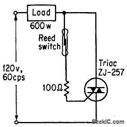
TRIAC_REED_A_C_SWITCH
Published:2009/7/24 4:27:00 Author:Jessie


Gale-controlled semiconductor switch (GE Triac) and magnetic reed switch provide on-off ac switching with minimum components. Gate signal of 3 V at 50 ma, either polarity, triggers Triac for handling 600.W load.-M. P. South. worth, Bidirectional Static Switch Simplifies Ac Control, Control Engineering, March 1964, p 75-16. (View)
View full Circuit Diagram | Comments | Reading(2338)
Simple_level_detector_using_a_comparator
Published:2009/7/24 4:27:00 Author:Jessie
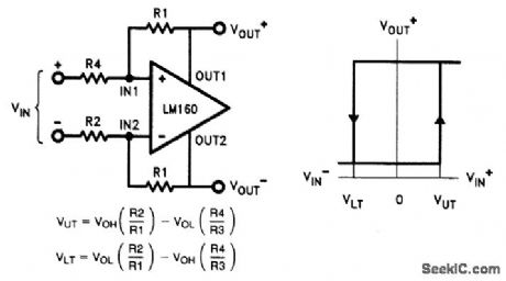
Fig. 15-13 This circuit shows how a high-speed comparator (LM160) can be used as a level detector or line receiver. The hysteresis graph and equations show the relationship between input and output voltages.National Semiconductor Linear Applications Handbook. 1991. p. 326. (View)
View full Circuit Diagram | Comments | Reading(879)
DUAL_51_V_SWITCHING_POWER_SUPPLY
Published:2009/7/24 4:27:00 Author:Jessie
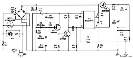
The ac voltage taken from PL1 feeds into bridge rectifier BR1, which delivers a full-wave output of approximately 165 Vdc.The network composed of R1, R2, D1, D3, and D4 generates a series of 5-V pulses that perform two important functions: First, the pulses are used as a 5-V power source for the pulse shaping and monostable network through D2 and C1. Second, the pulses trigger optoisolator IC1 and power triac TR1 via the pulse-shaping network, composed of Q1, Q2, and R3 to R5, and the mono-stable circuit, made of C2 and R6. Resistor R2 sets the maximum pulse width and, therefore, the maximum output voltage. With-out feedback, the unfiltered peak voltage is approximately 90 V. To obtain the required 51-V output, the feedback network (composed of R6, R7, and C3) reverse-biases the optoisolator whenever the output voltage exceeds 51 V. That, then forces TR1 Lo turn off as the unfiltered voltage goes to 0 V. The RC feedback network, therefore, regulates the output voltage by actively modifying IC1's conducting state. Resistor R8 limits the current through the optoisolator, and C4 and R9 ensure that the optoisolator's operation is stable and safe. Also, R10 limits surge current through TR1 when the supply is first turned on. Capacitors C5 and C6, along with R10, form a low-pass filter stage that minimizes ripple current. Resistor R11 discharges C5 and C6 when the power supply is turned off. (View)
View full Circuit Diagram | Comments | Reading(979)
Paralleling_three_terrninal_regulators
Published:2009/7/24 4:27:00 Author:Jessie
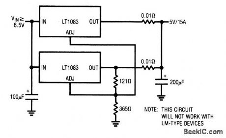
This circuit shows to use two three-terminal regulators to achieve and output current equal to the sum of the regulators. The circuit capitalizes on the 1 % output tolerance of the specified regulators to produce a simple parallel configu-ration. Both regulators sense from the same divider string. The series-output resistors provide ballast to account for the slightly differing output voltages. This added impedance degrades total drcuit regulation to about 1%. (View)
View full Circuit Diagram | Comments | Reading(1798)
FM_tuner_with_single_tuned_detector_coil
Published:2009/7/24 4:33:00 Author:Jessie
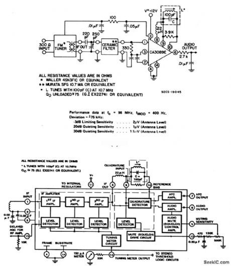
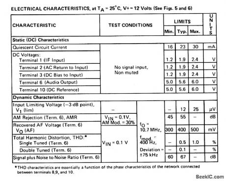
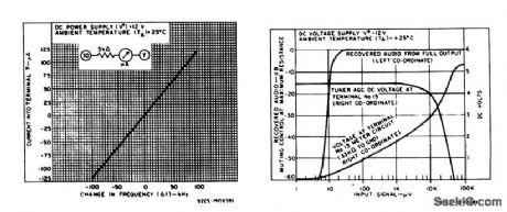
The CA3089 shown in this circuit includes an IF amplifier, quadrature detector, AF preamplifier, and specific circuits for AGC, AFC, muting (squelch), and tuning meter, as shown in Fig. 2-60B. Limiting sensitivity is 12μV (typical) at -3-dB point. The recovered audio is a typical 400 mV. Distortion (with a double-tuned coil) is a typical 0.1%. Typical characteristics are shown in Fig.2-60C. (View)
View full Circuit Diagram | Comments | Reading(1057)
VIDEO_TAPE_PREAMP
Published:2009/7/24 4:33:00 Author:Jessie
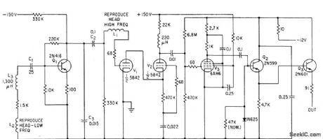
Two windings on reproduce head extend frequency response to 1 Mc. Winding L2 is connected conventionally to input of Q1; when transistor gain drops off at higher frequencies, L1 at input of first tube takes over. Preamp output to 91-ohm line is 1.5 V peak to peak.-G. N. Johnson, W. R. Johnson, and J. T. Mullin, Magnetic Recorder Response, Electronics, 34:10, p 186-188. (View)
View full Circuit Diagram | Comments | Reading(1009)
Extending_three_terminal_regulator_current_capability_sznitch_mode
Published:2009/7/24 4:32:00 Author:Jessie

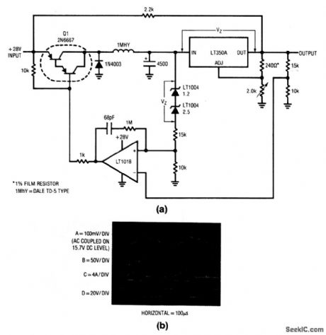
In this circuit, the LT350A functions in the normal manner and supplies a regulated output at 3-A capacity. The remaining components form a switch-mode dissipation-limiting control. This loop forces the potential across the LT350A to equal the 3.7-V value of VZ. When the input of the regulator (trace A, Fig. 9-9B) decays far enough, the LT1018 output (trace B) switches low and turns on Q1 (Q1 collector is trace D). This allows current flow (trace C) from the circuit input into the 4500-μF capacitor and raises the regulator input voltage. When the regulator input rises far enough, the comparator goes high, Q1 cuts off, and the capacitor ceases charging. Despite changes in input voltage, different regulated outputs or load shifts, the switch-mode loop ensures minimum possible dissipation in the regulator. (View)
View full Circuit Diagram | Comments | Reading(1178)
DELAY_LINE_PULSES_FOR_VIDEO_RECORDER
Published:2009/7/24 4:32:00 Author:Jessie
Blocking oscillator arrangement gives 0.3 microsec pulse length for recording by time-division multiplexing of S2 channels on two-track video recorder, and 0.8 microsec pulses when S1 is set for playback.-M. H. Damon and F. J. Messina, High-Density Storage of Wideband Analog Data, Electronics, 35:13, p 45-49. (View)
View full Circuit Diagram | Comments | Reading(1182)
Simple_zero_crossing_detector
Published:2009/7/24 4:32:00 Author:Jessie
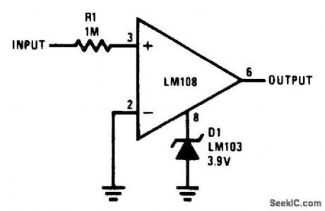
Fig. 15-17 This circuit uses an LM108 op amp as a voltage comparator to produce a simple zero-crossing detector. The output is clamped so that the circuit can drive DTL or TTL directly. National Semiconductor Linea Applications Handbook 1991, p. 71. (View)
View full Circuit Diagram | Comments | Reading(2016)
Using_a_timer_as_a_comparator
Published:2009/7/24 4:31:00 Author:Jessie

Fig. 15-16 This circuit uses an LM122 timer as a comparator with adjustable threshold levels. The output can be inverted or noninverted, as selected by a switch (or permanent wiring). Using the values shown and a +5-V supply, the threshold can be set between 0 and 3 V. National Semiconductor, Linear Applications Handbook, 1991, p. 335. (View)
View full Circuit Diagram | Comments | Reading(765)
225_to_400_MHz_60_W_amplifier_28_V_supply
Published:2009/7/24 4:31:00 Author:Jessie
This amplifier can be used as is or two amplifiers can be combined with quadrature-couplers to form a 100-W amplifier. Figure 2-59B shows the construction details for transformers T1/T2, Figures 2-59C and 2-59D show the component layout, and PC-board layout, respectively. Figures 2-59E, 2-59F, and 2-59G show typical amplifier performance characteristics. Those not familiar with microstrip techniques (for Z1 through Z5) should read the many Motorola publications,such as AN548A and AN555. (View)
View full Circuit Diagram | Comments | Reading(770)
SIMPLE_DUAL_VOLTAGE_POWER_SUPPLY
Published:2009/7/24 4:31:00 Author:Jessie
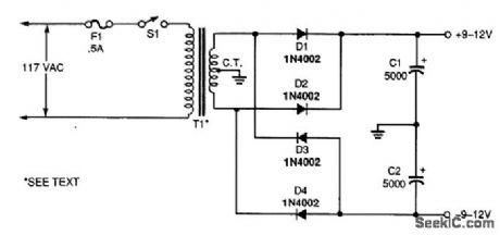
This circuit can be used to power op-amp circuits or other applications that require dual plus and minus supplies. This is a most basic circuit and is not regulated. T1 is a 120:12-V transformer of 100 mA (or more) capacity. (View)
View full Circuit Diagram | Comments | Reading(722)
| Pages:1192/2234 At 2011811182118311841185118611871188118911901191119211931194119511961197119811991200Under 20 |
Circuit Categories
power supply circuit
Amplifier Circuit
Basic Circuit
LED and Light Circuit
Sensor Circuit
Signal Processing
Electrical Equipment Circuit
Control Circuit
Remote Control Circuit
A/D-D/A Converter Circuit
Audio Circuit
Measuring and Test Circuit
Communication Circuit
Computer-Related Circuit
555 Circuit
Automotive Circuit
Repairing Circuit