
Circuit Diagram
Index 1195
Comparator_oscillator_clock_generator
Published:2009/7/24 4:56:00 Author:Jessie
Fig, 15-36 This self-starting fixed-frequency oscillator gives excellent frequency stability. The frequency is determined by R1/C1, and R2 provides the regenerative feedback. D1 enhances the stability by compensating for the difference between VOH and VSUPPLY. In applications where a precision clock generator up to 100 kHz is required, such as in automatic test equipment, C1 can be replaced by a crystal. Figures 15-32B and 15-32C show the pin connections and electrical characteristics, respectively. Harris Semiconductor. Linear & Telecom ICs, 1991, p. 4-30. (View)
View full Circuit Diagram | Comments | Reading(760)
DIGITAL_DATA_WRITE_AMPLIFIER
Published:2009/7/24 4:55:00 Author:Jessie
Delivers 8-ma swing to record head. Rise time is 15 millisec, sufficient for nonreturn-to-zero re cording at 20 kc, using head with 50-mh inductance. Carrier-type amplifier overcomes usual stability and level problems associated with d-c amplifiers.-R. F. Shaw, Universal Tape Amplifiers for Digital Data Systems, Electronics, 31:41, p 91-93. (View)
View full Circuit Diagram | Comments | Reading(826)
Fast_window_detector
Published:2009/7/24 4:55:00 Author:Jessie
Fig. 15-35 Because of its speed, low offset current, and low offset voltage, this circuit is ideal for industrial-process system-feedback controllers or out-of-limit alarm indicators. The output indicates that the input is within the high-reference and low-reference window. Figures 15-32B and 15-32C show the pin connections and electrical characteristics, respectively. Harris Semiconductor Linear & Telecom ICs, 1991, p. 4-30. (View)
View full Circuit Diagram | Comments | Reading(766)
SHOCKLEY_DIODE_MVBR_TESTS_TRANSPORTS
Published:2009/7/24 4:54:00 Author:Jessie
For testing tape transports, frequency can be varied over 15:1 range and mark/space ratio from 1:15to 15:1. Shockley diodes MR1 and MR2 serve as changeover switch. Two additional diodes, at MR3 and MR4, are needed if reverse voltage rating of diodes is less than their striking voltage.-C. J. Dakin, Novel Multivibrators Test Tape Transports, Electronics, 37:7, p 40-43. (View)
View full Circuit Diagram | Comments | Reading(1015)
Comparator_RS232_to_CMOS_line_receiver
Published:2009/7/24 4:54:00 Author:Jessie
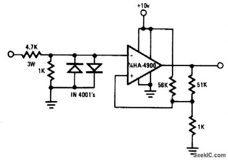
Fig. 15-34 This RS232-type line receiver to drive CMOS logic uses a Schmitt-trigger feedback network to provide about 1-V input hysteresis for added noise immunity. The diodes and input resistor minimize transient spikes when the interface connection is made or broken. Figures 15-32B and 15-32C show the pin connections and electrical characteristics, respectively. Harris Semiconductor, Linear & Telecom ICs 1991, p. 4-30. (View)
View full Circuit Diagram | Comments | Reading(732)
DIGITAL_DATA_READ_AMPLIFIER
Published:2009/7/24 4:53:00 Author:Jessie
Presents 10,000-ohm input impedance to read head. No-signal input produces -4 V output; peak input as low as 1.35 my zero-to-peak produces +4 v output. Gives satisfactory reading at pulse repetition rates up to 22 kc.-R. F. Shaw, Universal Tope Amplifiers for Digital Data Systems, Electronics, 31:41, p 91-93. (View)
View full Circuit Diagram | Comments | Reading(649)
Comparator_logic_level_translator_CMOS_to_TTL
Published:2009/7/24 4:53:00 Author:Jessie
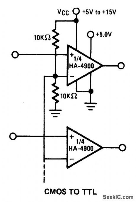
Fig. 15-33 This circuit is similar to that of Fig. 15-32, except that the interface is from CMOS to TTL. Harris Semiconductor linear & Telecom ICs 1991, p. 4-29. (View)
View full Circuit Diagram | Comments | Reading(880)
ERASE_AND_BIAS_OSCILLATOR
Published:2009/7/24 4:53:00 Author:Jessie
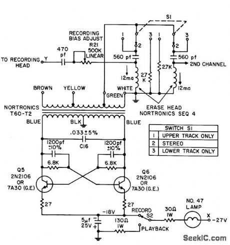
Provides ample power for 60 db erasure of saturated tape, using 10 ma of 80-kc erase signal. Total power output is 1.5 W at efficiency of 60%. Bias current is same frequency.- Transistor Manual, Seventh Edition, General Electric Co., 1964, p 278. (View)
View full Circuit Diagram | Comments | Reading(1797)
110__to_220_V_regulation_without_switching
Published:2009/7/24 4:52:00 Author:Jessie
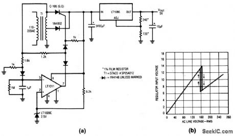
This circuit allows a voltage-regulator to operate on a 110- or 220-V line without having to switch transformer windings. When T1 is driven from 110 V, the LT1011 output goes high and allows the SCR to receive gate bias through the 1.2-kΩ resistor. The 1N4002 is off. T1 output is rectified by the SCR and the regulator sees about 8.5 V at the input. If T1 is plugged into 220 V, the inverting input at the LT1011 is driven beyond 2.5 V, and pin 7 clamps low. This steers the SCR gate bias to ground through the LT1011. The diodes at the LT1011 output prevents reverse voltages from reaching the SCR or the LT1011 output. The SCR goes off and the 1N4002 sources current to the regulator from the T1 center tap. Although the T1 input voltage has doubled, the T1 output is cut in half and regulator power dissipation remains the same. Figure 9-14B shows ac line input versus regulator input-voltage transfer. The switch to center-tap drive occurs midway between 110 and 220 V. (View)
View full Circuit Diagram | Comments | Reading(1159)
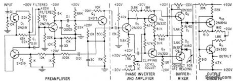
COMPRESSOR
Published:2009/7/24 4:52:00 Author:Jessie
Has unity gain, expansion of 3 db, and compression of 12 db. Gain adjustments are automatic, Used to maintain even recording level during tape-recorded interviews.-E. C, miller, Audio Volume Compressor, Electronics, 33:2, p 62. (View)
View full Circuit Diagram | Comments | Reading(0)
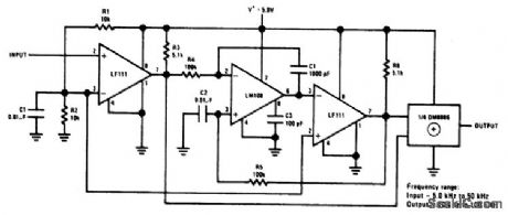
EMITTER_COUPLED_RC_OSCILLATOR
Published:2009/7/1 2:34:00 Author:May
The circuit covers 15 Hz-30 kHz and is useful as a function generator. The 2N2926 or equivalent transistors can be used. (View)
View full Circuit Diagram | Comments | Reading(861)
150_TO_300_MHz_DOUBLER
Published:2009/7/1 2:33:00 Author:May
View full Circuit Diagram | Comments | Reading(571)
FREQUENCY_DOUBLER
Published:2009/7/1 2:32:00 Author:May
View full Circuit Diagram | Comments | Reading(2466)
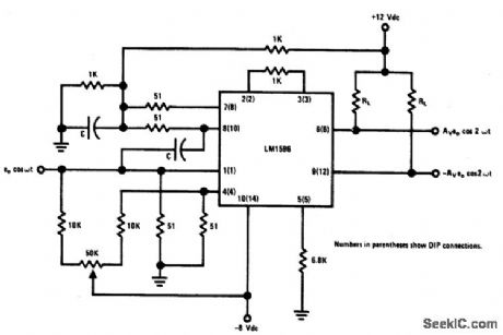
PROGRAMMABLE_VOLTAGE_CONTROLLED_FREQUENCY_SYNTHESIZER
Published:2009/7/1 2:32:00 Author:May
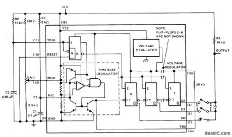
The μA2240 consists of four basic circuit elements: (1) a time-base oscillator, (2) an eight-bit countqr, (3) a control flip-flop, and (4) a voltage regulator. The basic frequency of the time-base oscillator (TBO) is set by the external time constant determined by the values of R1 and C1 (R1C1 = 2 kHz). The open-collector output of the TBO is connected to the regulator output via a 20 k ohm pull-up resistor, and drives the input to the eight-bit counter. At power-up, a positive trigger pulse is detected across C2 which starts the TB0 and sets all counter outputs to a low state. Once the μA2240 is initially triggered, any further trigger inputs are ignored until it is reset. In this astable operation, the μA2240 will free-run from the time it is triggered until it receives an external reset signal. Up to 255 discrete frequencies can be synthesized by connecting different counter outputs. (View)
View full Circuit Diagram | Comments | Reading(640)
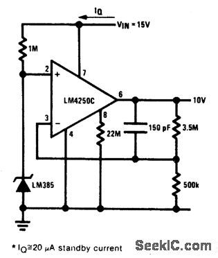
PRECISION_REFERENCE_MICROPOWER_10_V_REFERENCE
Published:2009/7/1 2:30:00 Author:May
View full Circuit Diagram | Comments | Reading(579)
Switch_bounce_eliminator_or_filter
Published:2009/7/24 5:28:00 Author:Jessie
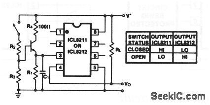
This circuit provides a rapid charge-up of C1 to near V+ on switch closure, and a corresponding slow discharge of C1 on switch break. By proportioning the time constant of R1/C1 to approximately the manufacturer's rated bounce time, the output at terminal 4 of the ICL8211/12 will be a single change of state (no bounce) per switch closure, as shown by the table. (View)
View full Circuit Diagram | Comments | Reading(916)
BROADBAND_FREQUENCY_DOUBLER
Published:2009/7/1 2:29:00 Author:May
Circuit Notes
This circuit will double lowlevel signals with low distortion. The value of C should be chosen for low reactance at the operating frequency. Signal level at the carrier input must be less than 25 mV peak to maintain operation in the linear region of the switching differential amplifier. Levels to 50 mV peak may be used with some distortion of the output waveform. If a larger input signal is available, a resistive divider may be used at the carrier input with full signal applied to the signal input. (View)
View full Circuit Diagram | Comments | Reading(1041)
High_resolution_continuous_output_sampled_bridge
Published:2009/7/24 5:28:00 Author:Jessie
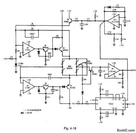
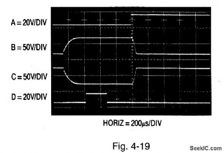
Figure 4-18 shows a sampled bridge with continuous output and high resolution.Figure 4-19 shows the waveforms. Traces A, B, C, and D show the A1A output, Q3 emitter, complementary output to A2 loop, and the 74C221 delayed pulse to Q5.The circuit applies 100 V across a 10-V, 350-0 strain-gauge bridge for short periods of time. The high pulsed-voltage drive increases bridge output proportionally, without forcing excessive dissipation. The average bridge power is far below the normal 29 mA obtained with the usual 10-Vdc excitation. Combining the 10× higher bridge gain (300 mV full-scale versus the normal 30 mV) with a chopper-stabilized amplifier in the sample-hold output stage is the key to the high resolution. To calibrate, simply adjust the 50-kΩ zero control for zero output with the bridge at mechanical zero. Although the output is continuous, information is collected at a 1-Hz rate, and the Nyquist limit applies when interpreting results. LINEAR TECHNOLOGY, APPLICATION NOTE 43, P. 23. (View)
View full Circuit Diagram | Comments | Reading(723)
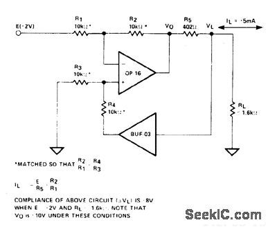
INVERTING_BIPOLAR_CURRENT_SOURCE_HIGH_SPEED
Published:2009/7/1 2:29:00 Author:May
View full Circuit Diagram | Comments | Reading(714)
Offline_flyback_converter_
Published:2009/7/24 5:27:00 Author:Jessie
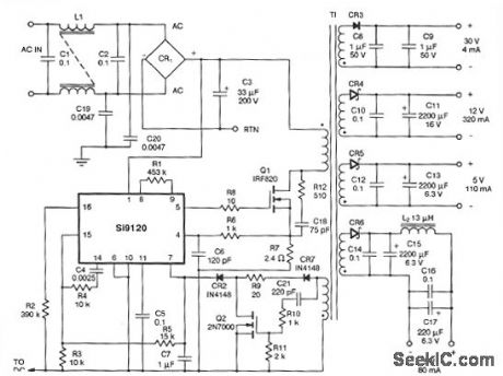
This circuit operates from 90-to 130-V .Regulation is 5% on all output .Ripple is 200 mV p-p on the +30 and +12 outputs ,50 mVp-p on the main +5 output,15 mVp-p on the auxiliay +5 output. power consumptions is 15W.T1 is a Schott Corp.#6712244, L1 is any 8mH common-mode choke, L2 is a Magnetics Inc J40401TC with 6 turn #26 AWG ,and CR1 is any 1-A 600-V bridge. (View)
View full Circuit Diagram | Comments | Reading(2784)
| Pages:1195/2234 At 2011811182118311841185118611871188118911901191119211931194119511961197119811991200Under 20 |
Circuit Categories
power supply circuit
Amplifier Circuit
Basic Circuit
LED and Light Circuit
Sensor Circuit
Signal Processing
Electrical Equipment Circuit
Control Circuit
Remote Control Circuit
A/D-D/A Converter Circuit
Audio Circuit
Measuring and Test Circuit
Communication Circuit
Computer-Related Circuit
555 Circuit
Automotive Circuit
Repairing Circuit