
Circuit Diagram
Index 1212
SERIES_SCR_LAMP_FLASHER_HANDLES_A_WIDE_RANGE_OF_LOADS
Published:2009/6/30 22:56:00 Author:May
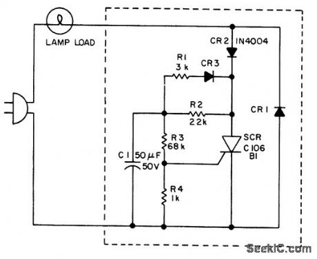


Brief full-power flashes are obtained when the SCR conducts during positive half cycles of the line voltage. The SCR fires when the voltage at the divider, R3 and R4, reaches the gate-firing level. Diode D1 conducts during the reverse cycle of the SCR and provides preheating current to the lamp filaments.
(View)
View full Circuit Diagram | Comments | Reading(769)
BEAT_FREQUENCY_DISPLAY
Published:2009/6/30 22:55:00 Author:May
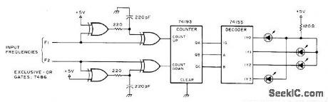
Apparent rotation of dot on four-LED display gives indication of beat frequency between ttnro tone oscillators.When F1 is greater than F2, dot rotates clockwise. When F1 is less than F2, dot rotates coun torclockwise. When F1 equals F2, dot does not move.-Circuits, 73Magazine, July 1977, p 35. (View)
View full Circuit Diagram | Comments | Reading(910)
6-DIGIT_WITH_CALENDAR_AND_ALARMS
Published:2009/6/30 22:55:00 Author:May

Circult is built around Cal-Tex CT7001 IC that includes outputs for displaying day of monthalong with time on Liftonix DL707 LED read-outs. Transistor switch Q1 and relay form timer triggered by IC to control radio or other appli-ance drawing up to 5 A from AC Iine. Dual-volt-age power supply provideg 7 and 14 VDC. Includes snooze alarm along with regular built-intransistor-driven buzzer.-M. s. Robbins, Electronic Clocks and Watches, Howard W.Sams, Indianapolis,IN,1975,p 103-104 and116-117. (View)
View full Circuit Diagram | Comments | Reading(1337)
CMOS_DATA_ACQUISITION_SYSTEM
Published:2009/6/30 22:50:00 Author:May
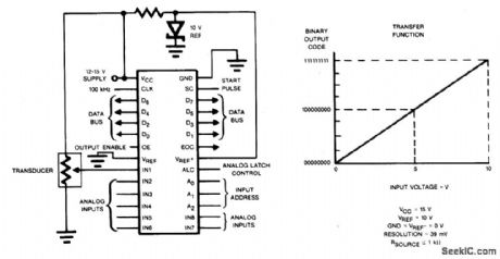
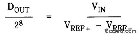
Charge redistribution to achieve A/D conversion. In typical applications, as a ratiometric conversion system for a microprocessor,VREF- will be connected to ground and VREF,+will be connected to VCC. The output will then be a simple proportional ratio between analog input voltage and VCC. The general relationship is:
Where DOUT=Digital Output VIN=Analog Input VREF=Positive Reference Potential VREF= Negative Reference Potential (View)
View full Circuit Diagram | Comments | Reading(818)
12_h_WITH_SECONDS
Published:2009/6/30 22:49:00 Author:May
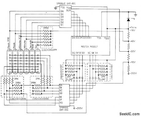
Combination of Mostek clock IC and Sprague high-voltage display drivers, acting through 206C and 216C single in-line resistor network, provides drive for conventional seven-element gas-discharge digital clock display showing hours, minutes, and seconds. Requires -200 V supply. Display can be Burroughs Panaplex, Cherry Plasma-Lux, or Beckman SP series.- Integ rated Circuits Data book-1, Sprague, North Adams, MA 1978, p 3-5.
(View)
View full Circuit Diagram | Comments | Reading(1704)
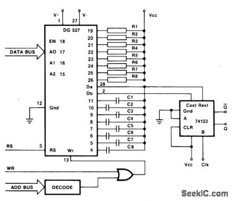
8048_IM8OC48_MICROCOMPUTER_WITH_8_CHARACTER16_SEGMENT_ASCII_TRIPLEX_LIQUID_CRYSTAL_DISPLAY
Published:2009/6/30 22:47:00 Author:May
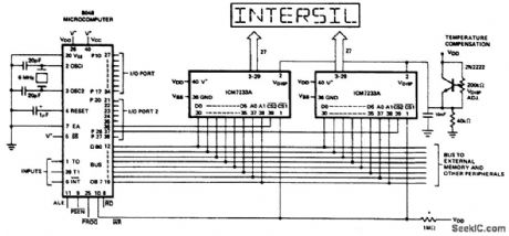
The two bit character address is merged with the data and written to the display driver under the control of the WR line. Port lines are used to either select the target driver, or deselect all of them for other bus operations. (View)
View full Circuit Diagram | Comments | Reading(1028)
HIGH_POWER_BATTERY_OPERATED_FLASHER
Published:2009/6/30 22:46:00 Author:May
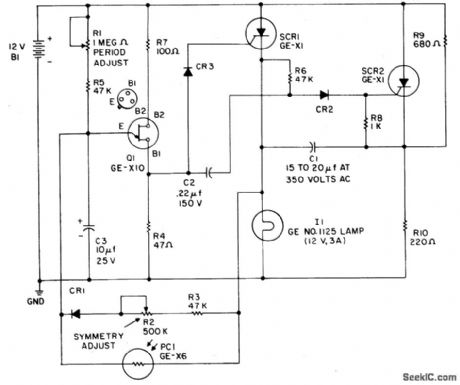
This flasher operates from a 12-volt car or boat battery. It offers 36 to 40-watts output, variable flash rate (up to 60 flashes per minute), independent control of both on and off cycles and photoelectric night and day control that turns the flasher on at night and shuts it off during the day for automatic operation. SCR1 and SCR2 form a basic dc flip-flop. The lamp load is the cathode leg of one SCR so that the other side of the load may be at ground (negative) potential (required in some applications). The flip-flop timing is controlled by a conventional UJT oscillator arrangement (Q1, R1, C3, etc.). Potentiometer R2 and diode CR1 provide on/off timing independence. Photoconductor PC1 locks out the UJT firing circuit during the daylight hours. (View)
View full Circuit Diagram | Comments | Reading(672)
TIDE_CLOCK
Published:2009/6/30 22:46:00 Author:May
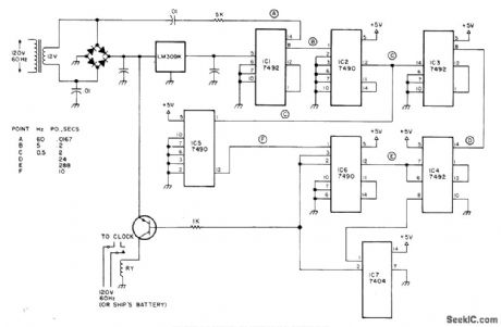
Circuit shuts off electric clock of any type for 5 s out of every 144 s, to give loss of 50 min in 24 h as required for making high tides conform to clock readings. Regulated 5-V supply shown drives TTL 7492 frequency divider that reduces 60-Hz line frequency by factor of 12 to 5 Hz. 7490 divides this by 10 to give 0.5 Hz.Two more 7492s divide by 12 and 12 to give symmetrical pulses with period of 288s. Second 7490 divides 2-s pulse down to 10 s. Counter IC4 inhibits 5-s counter by feeding low output into one gate of IC7 hex inverter. When IC4 counts up to 144 s, its output goes high and resets IC6 to low for start of 5-s low period of that counter.Article gives timing waveforms. Switching tran-sistor is used to control relay that opens clock circuit. Set tide clock at 12:00 for high tide at location of use .and t will be 12:00 at high tide thereafter.Low tide will then be at 6:00.-J.F.Crowhter Time and -Digitally,73 magazine,Aug.1978,p 156-157 (View)
View full Circuit Diagram | Comments | Reading(1593)
MICROPROCESSOR_SELECTED_PULSE_WIDTH_CONTROL
Published:2009/6/30 22:44:00 Author:May
Differential multiplexers are generally used in process control applications to eliminate errors due to common mode signals. In this circuit however, advantage is taken of the dual multiplexing capability of the switch. This is achieved by using the multiplexer to select pairs of RC networks to control the pulse width of the multivibrator. This can be a particularly useful feature in process control applications where there is a requirement for a variable width sample window for different control signals. (View)
View full Circuit Diagram | Comments | Reading(665)
ELECTRONIC_LIGHT_FLASHER
Published:2009/6/30 22:44:00 Author:May
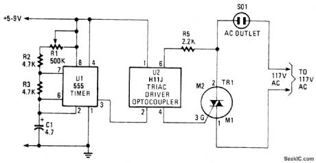
The blinking or flashing rate is determined by U1, a 555 timer integrated circuit. Its output, at pin 3, feeds U2, a HIIJ triac driver. That driver consists of an infrared LED that is coupled internally to a light-activated silicon bilateral switch (DIAC). When the LED internal to U2 is turned on by the timer, U1, its light triggers the DIAC; effectively closing the circuit between pins 4 and 6, and fires the Triac, TRI through its gate circuit. When the Triac is firing, it acts as a closed circuit that turns on the light (or other device it may be controlling via 501). When the timer turns off, the LED, the DIAC and Triac stop conducting and the light turns off. The sequence then repeats. The flashing rate can be varied by means of R1, a 500,000 ohm potentiometer. (View)
View full Circuit Diagram | Comments | Reading(3727)
EIGHT_CHANNEL_MUX_DEMUX_SYSTEM
Published:2009/6/30 22:40:00 Author:May
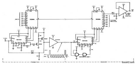


A number of signals may be sent between two points simultaneously by making a slight modification in the receiver circuit. A second DG508A is used as a demultiplexer, allowing all 8 channels to be monitored continuously. (View)
View full Circuit Diagram | Comments | Reading(671)
ALTERNATING_FLASHER
Published:2009/6/30 22:39:00 Author:May

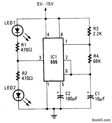
The LED's flash alternately.The flash rate is determined by C1 and R4. (View)
View full Circuit Diagram | Comments | Reading(2150)
LCD_WRISTWATCH
Published:2009/6/30 22:38:00 Author:May
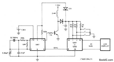
Inverter section of Intel 5801 oscillator/divider is used with 32,768-Hz crystal to produce time base. First divider in 5801 reduces this to 1024 Hz for driving upcon-verter transistor. Feedback from transistor through 12-V zener is used to regulate and con-trol pulse width of 1024-Hz signal. Upconverter also provides 12-15 V required by LCD and 5201 decoder/driver IC. Output to each LCD segment and to common backplate is 32-Hz square wave.Separate drive flashes colon at 1-Hz rate.-M. S. Robbins, Electronic Clocks and Watches, Howard W, Sams, Indianapolis, IN, 1975, p 128-130. (View)
View full Circuit Diagram | Comments | Reading(1418)
MINIATURE_TRANSISTORIZED_LIGHT_FLASHER
Published:2009/6/30 22:36:00 Author:May
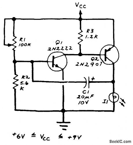
R1 adjusts the flash rate. The lamp should be a No. 122, No. 222 or other similar, miniature incandescent lamp. (View)
View full Circuit Diagram | Comments | Reading(673)
PRF_MONITOR_UPPER
Published:2009/6/30 22:35:00 Author:May
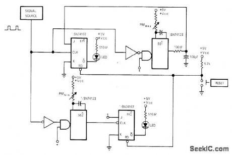
Upper channel latches when pulse repetition frequency of train of pulses is higher than specified limits,turning on abovelimit LED driven by JK fip-flop FF1. Lower channel latches and turns on its LED when PRF is below second specified limit, Upper channel als detects single noise pulse,while lower channel detects single missing pulse,After offlimit indication,circuit must be reset.-L.Bilkwood and D.Porat、PRF Monitor with Adjustable End Limits、EDN/EE Magazine,Feb.1、1972,p57-58
(View)
View full Circuit Diagram | Comments | Reading(735)
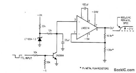
Vpp_GENERATOR_FOR_EPROMS
Published:2009/6/30 22:34:00 Author:May
View full Circuit Diagram | Comments | Reading(699)
LOW_VOLTAGE_LAMP_FLASHER
Published:2009/6/30 22:32:00 Author:May
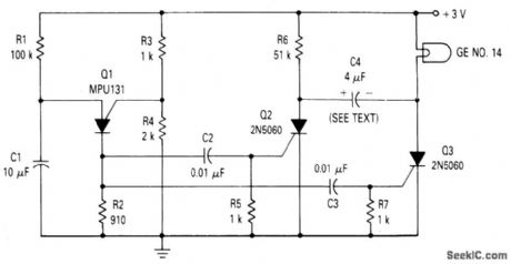
The circuit is composed of a relaxation oscillator formed by Q1 and an SCR flip-flop formed by Q2 and Q3. With the supply voltage applied to the circuit, the timing capacitor C1 charges to the firing point of the PUT, 2 volts plus a diode drop. The output of the PUT is coupled through two 0.02 μF capacitors to the gate of Q2 and Q3. To clarify operation, assume that Q3 is on and capacitor C4 is charged plus to minus as shown in the figure. The next pulse from the PUT oscillator turns Q2 on. This places the volt-age on C4 across Q3 which momentarily reverse biases Q3. This reverse voltage turns Q3 off. After discharging, C4 then charges with its polarity reversed to that shown. The next pulse from Q1 turns Q3 on and Q2 off. Note that C4 is a non-polarized capacitor. For the component values shown, the lamp is on for about 1/2 second and off the same amount of time. (View)
View full Circuit Diagram | Comments | Reading(868)
8_BIT_μP_BUS_INTERFACE
Published:2009/6/30 22:28:00 Author:May

with this double latch technique,valid data will be latched to the DAC until updatedwith the E2 pulse,Timing Will depend on the processor used。 (View)
View full Circuit Diagram | Comments | Reading(660)
AGC_WITH_FET
Published:2009/6/30 22:25:00 Author:May
FET serves as nonlinear element in fastacting instrumentation circuit han-dling wide range of signals. R1 and R2 attenuate input signal so FET input is less than 25 mV for inputs up to 2 VRMS. Article covers design and performance. Gain is almost linear with gate voltage of FET,-R D Pogge,Designers'Guide to:Basic AGC Amplifier Design、EDNMagazine,Jan,20、1974、p 72-76 (View)
View full Circuit Diagram | Comments | Reading(1185)
AGC_AMPLIFIER
Published:2009/6/30 22:24:00 Author:May
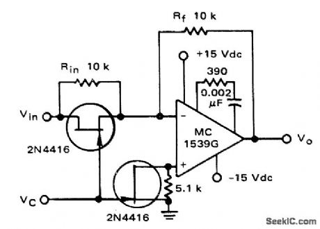
FET used in conjunction with opamp permits varying of gain by changing ratio of Rf to Rin. Offset voltage in output due to input bias currents is minimized by placing FET in parallel with 5.1K resistor between noninverting leg of opamp and ground, so resistance varies with changes of It,,- Low Frequency Applications of Field-Effect Transistors, Motorola, Phoenix, AZ, 1976, AN-511A, p 9. (View)
View full Circuit Diagram | Comments | Reading(2203)
| Pages:1212/2234 At 2012011202120312041205120612071208120912101211121212131214121512161217121812191220Under 20 |
Circuit Categories
power supply circuit
Amplifier Circuit
Basic Circuit
LED and Light Circuit
Sensor Circuit
Signal Processing
Electrical Equipment Circuit
Control Circuit
Remote Control Circuit
A/D-D/A Converter Circuit
Audio Circuit
Measuring and Test Circuit
Communication Circuit
Computer-Related Circuit
555 Circuit
Automotive Circuit
Repairing Circuit