
Index 90
GENERIC_TRIAC_SWITCH_INTERFACE_FOR_INDUCTIVE_LOAD
Published:2009/7/16 23:26:00 Author:Jessie
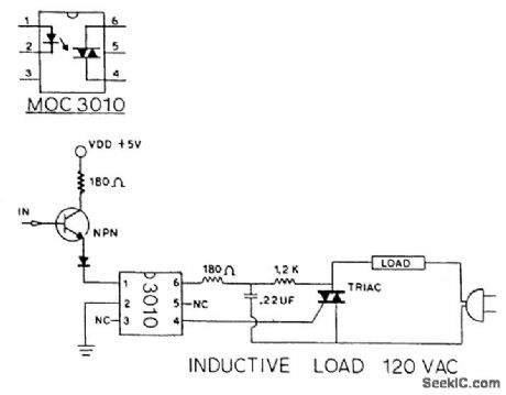
A TTL level input turns on the MOC3010 optocoupler and triggers the triac, applying 120 Vac to the load. (View)
View full Circuit Diagram | Comments | Reading(3940)
±15_V_TRACKING
Published:2009/7/16 23:25:00 Author:Jessie

Uses Motorola dual-polarity regulator to provide balanced positive and negative voltages, with series-pass transistor handling major part of output current. Developed for use with audio signal generator.- H. Olson, Integrated-Circuit Audio Oscillator, Ham Radio, Feb. 1973, p 50-54. (View)
View full Circuit Diagram | Comments | Reading(0)
PHOTOVOLTAIC_ISOLATOR_WITH_FAST_RESET_1
Published:2009/7/16 23:23:00 Author:Jessie
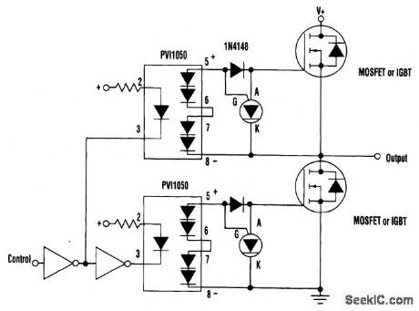
The combination of a weak photovoltaic isolator pull-up and a strong programmable junction transistor pull-down leads to a very simple half-bridge FET or IGBT driver, which virtually guarantees that the devices won't crowbar the power supply. The device turning off will do so rapidly, but the device turning on will do so very slowly. A dead time is inherent in the circuit dynamics, so no additional circuitry is required to prevent a crowbar or shoot-through effect. (View)
View full Circuit Diagram | Comments | Reading(3439)
IMPROVED_ULTRA_LONG_MONO
Published:2009/7/16 23:21:00 Author:Jessie
Eliminayion of reset transistor and coupling diode makes circuit insensitive to supply bus transients, cuts standby current to essentially zero, and improves efficiency under heavy loading. Will handle loads above 150 ma.-J. C. Schaeffert and N. F. Goldman, Improved Ultra-Long Monosable Multivibrator, EEE, 12:12, p 57-58. (View)
View full Circuit Diagram | Comments | Reading(630)
PULSE_COINCIDENCE_DETECTOR
Published:2009/7/16 23:20:00 Author:Jessie
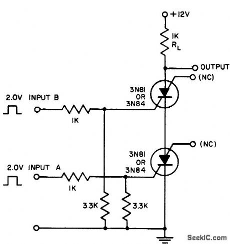
Provides output from silicon controlled switches only when input pulses are applied simultaneously at A und B, with 2 to 3 v amplitude. Over-lap of 1 microsec is sufficient for triggering.- Transistor Manual, Seventh Edition, General Electric Co., 1964, p 428. (View)
View full Circuit Diagram | Comments | Reading(2872)
PLATL_TO_GRID_COUPLED_MAIN_GATE_MVBR
Published:2009/7/16 23:20:00 Author:Jessie
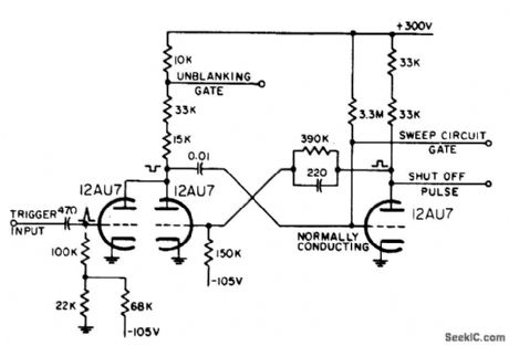
Triggered by connecting plate of trigger inverter or switch tube in parallel with plate of normally-off mvbr tube. Unblanking gate is generated at mvbr as negative output. Used in radar to provide pate during which display sweep is generated, together with gates for generating waveforms that must be coincident with display sweep.-NBS, Handbook Preferred Circuits Navy Aeronautical Electronic Equipment, Vol. 1, Electron Tube Circuits, 1963, p N10-2. (View)
View full Circuit Diagram | Comments | Reading(700)
RAIL_SPLITTER_VIRTUAL_GROUND_CIRCUIT
Published:2009/7/16 23:18:00 Author:Jessie
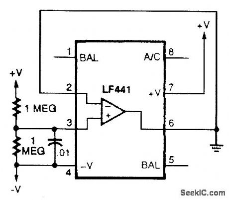
Use a low-power op amp, of which there are many to choose from. The National LF441 is a good, inexpensive choice (don't confuse it with the 411). Pin 6 is the virtual ground output. This circuit will work correctly down to a battery voltage of about 6V. The current consumption is about 160 μA. (View)
View full Circuit Diagram | Comments | Reading(2094)
12_V_AT_10_A_FOR_HOUSE
Published:2009/7/16 23:17:00 Author:Jessie

Power supply is more than adequate for handling 12-V FM transceiver and even small amplifier. Series combination of three 6.3-V 10-A filament transformers drives 12-A 50-PIV bridge rectifier supplying 18 VDC to National LM305 regulator and pass transistors. Output voltage is at least 4 V less. Circuit provides foldback-current limiting for protection against load shorts. 500-ohm pot varies output from 11.2 to 14.1 V. Q1 is 2N2905, Q2 is 2N3445, and Q3 is 2N3772. T1-T3 are 6.3 V at 10 A (Essex Stancor P-6464 or equivalent ).-C. Car-roll, That's a Big 12 Volts, QST, Aug. 1976, p 26-27. (View)
View full Circuit Diagram | Comments | Reading(3874)
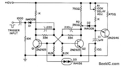
SPEEDING_ONE_SHOT_RECOVERY
Published:2009/7/16 23:16:00 Author:Jessie
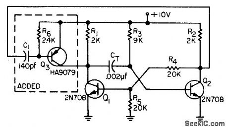
Additional transistor Q3 reduces charging time of timing capacitor, thereby increasing duty cycle. With values shown, circuit provides 10-microsec pulses with recovery time of 0.25 microsec, corresponding to repetition rate of almost 100,000 pps and 97.5% duty cycle.-W.A. Ross, Added Transistor Reduces One-Shot Recovery Time, EEE, 12:4, p 60. (View)
View full Circuit Diagram | Comments | Reading(770)
OP_AMP_CIRCUIT_DC_POWER_SUPPLY_CONNECTIONS
Published:2009/7/16 23:16:00 Author:Jessie
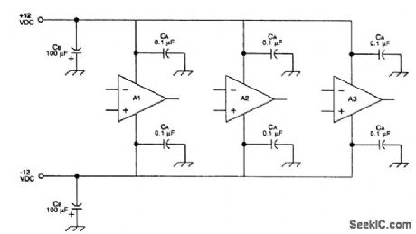
The dc power distribution of multistage, or multi-op-amp, filter circuits needs to be well conditioned to prevent either oscillation in one op amp or, because of poor power supply, decoupling between op amps. The figure shows the proper way to keep these problems under control. The capacitors marked CA are 0.1μF to 1μF, and must be mounted as close to the body as possible. A larger capacitor (marked CB), 100μF to 500μf, is connected between each power-supply line and ground, usually at the point of connection to the power supply. Note that these capacitors are polarity-sensitive; they must be connected into the circuit properly or they might be damaged. (View)
View full Circuit Diagram | Comments | Reading(1592)
FAST_RECOVERY_HYBRID_ONE_SHOT
Published:2009/7/16 23:15:00 Author:Jessie
Improved configuration provides wide timing range, good timing stability, and clean waveforms over extremely wide range of duty cycles. Can be retriggered immediately after completion of timing cycle without loss in overall timing accuracy.- Transistor Manual, Seventh Edition, General Electric Co., 1964, p 346. (View)
View full Circuit Diagram | Comments | Reading(657)
110_120_VAC_±_25_V_AT_600_W
Published:2009/7/12 22:21:00 Author:May
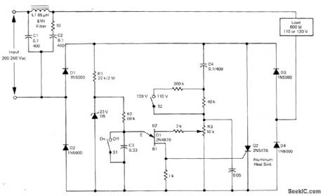
Simple openloop voltage compensator for small conduction angles operates from 200-260 VAC input and provides true RMS output voltage for sensitive equipment such as photographic enlargers,oven heaters, proiection lights, and certain types of AC motors. Full-wave bridge D1-D4 and SCR Q2 provide full-wave control, with UJT Q1 serving as trigger. Triggering frequency is determined by chargeand discharge of C3 through R2. As input voltage increases, required trigger voltage also increases, retarding firing point of SCR to compensate for change in input.-D.Perkins, True RMS Voltage Regulators, Motorola, Phoenix, AZ, 1975, AN-509, p 3. (View)
View full Circuit Diagram | Comments | Reading(1161)
28_V_AT_10_A
Published:2009/7/16 23:14:00 Author:Jessie
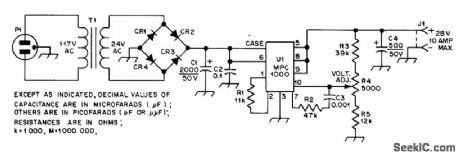
Developed for 60-W UHF linear amplifier. C1 and C4 are computer-grade electrolytics. CR1-CR4 are Motorola 1N3209 100-PIV 10-A silicon diodes. U1 is Motorola MPC100 or equivalent voltage regulator mounted on heatsink, T1 is Stancor P-8619 or equivalent 24-V 8-A transformer.-J. Buscemi, A 60-Watt Solid-State UHF Linear Amplifier, QST, July 1977, p 42-45. (View)
View full Circuit Diagram | Comments | Reading(795)
±15_V_AT_10_A_
Published:2009/7/16 23:13:00 Author:Jessie
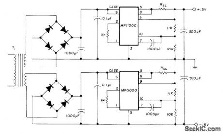
Uses two Motorola positive voltage regulators, each having separate 18-24 VRMS secondary winding on power transformer T1. Current-limiting resistor RSC is in range of 0.66 to 0.066 ohm. Use copper wire about 50% longer than calculated length and shorten step by step until required pass current is obtained; thus, start with 25 ft of No. 16, 15 ft of No. 18, 10 ft of No. 20, or 6 ft of No. 22.-G. L. Tater, The MPC1000-Super Regulator, Ham Radio, Sept. 1976, p 52-54. (View)
View full Circuit Diagram | Comments | Reading(1005)
VOLTAGE_FOLLOWER_STABILITY
Published:2009/7/16 23:12:00 Author:Jessie
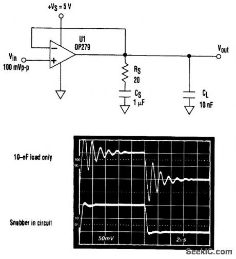
A unity-gain voltage follower driving a capacitive load is prone to stability problems. Using an RC snubber network (RS-RC) allows capacitive loads, such as CL to be compensated without loss of load drive.
The comparison of pulse response with and without the snubber network shows a dramatic reduction in overshoot. The top trace is without the snubber and the bottom trace is with the snubber. (View)
View full Circuit Diagram | Comments | Reading(1950)
LCD_AUXILIARY_BIAS_CIRCUIT
Published:2009/7/16 23:11:00 Author:Jessie
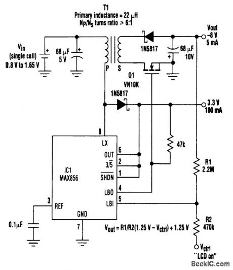
This single-cell boost converter can generate the low supply voltages commonly needed in pagers and other portable instruments with small, graphic LCDs. The first is a regulated 3.3 V at 100 mA, and the other is a regulated negative output, suitable for use as an LCD bias voltage. The overall efficiency is about 80 percent. The main 3.3-V supply is provided by a boost converter (IC1). The auxiliary bias voltage is provided by an extra flyback winding (the T1 secondary), and is regulated via Q1 and the low-battery detector internal to IC1. As the battery discharges, its declining terminal voltage causes a decline in the voltage in the flyback winding. At minimum battery voltage (0.8 V), the T1 primary sees 3.3 V-0.8 V2.5 V, so the 6:1 turns ratio produces 6(2.5)=15 V in the secondary. At maximum battery voltage (1.65 V), the primary sees only 1.5 V, producing 9.9 V in the secondary. MOSFET Q1 stabilizes this output by interrupting the secondary current, introducing the regulation necessary to generate a constant negative output. The regulator uses IC1's low-battery detector (a comparator/reference combination) as an on/off controller for Q1. In this circuit, the R1/R2 divider holds LB1 between Vctrl (normally 3.3 V) and the LCD bias output (normally -8 V). R1 and R2 are chosen so that LBO turns off when the LCD bias becomes too negative (and pulls the LB1 voltage below 1.25 V). Load current then causes the LCD bias to drift upward (toward 0 V) until LB1 exceeds 1.25 V, which causes Q1 to turn on again. A logic signal at the LCD ON terminal provides a means to enable and disable the negative output.
(View)
View full Circuit Diagram | Comments | Reading(1254)
_20_V_FOR_VARACTORS
Published:2009/7/16 23:11:00 Author:Jessie
Precision low-ripple bias supply for varactor tuning applications can provide up to 20-mA output current.-M. A. Chapman, Multiple Band Master Frequency Oscillator, Ham Radio, Nov. 1975, p50-55. (View)
View full Circuit Diagram | Comments | Reading(624)
2_TO_6_V_CCFL_POWER_SUPPLY
Published:2009/7/16 23:04:00 Author:Jessie
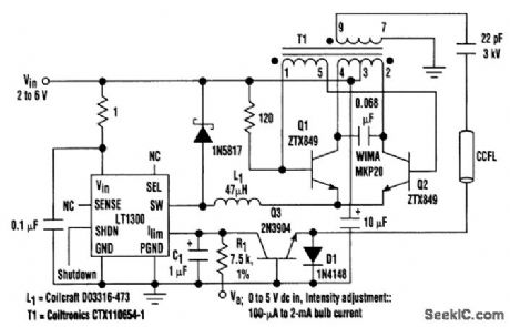
The power supply shown operates from 2 to 6 V. It can drive a small (75-mm) CCFL over a 100-μA to 2-mA range. An LT1301 micropower dc-to-dc converter is used in conjunction with a current-driven Royer-class converter, consisting of T1, Q1, and Q2. When power is applied along with intensity-adjust voltage Va, the LT1301's Ilim pin is driven slightly positive, causing maximum switching current through the IC's internal switch pin (SW). L1 conducts current that flows from transformer T1's center tap, through the transistors, into L1. L1's current is taken in switched fashion to ground by the regulator's action. The Royer converter oscillates at a frequency primarily set by T1's characteristics (including its load) and the 0.068-μF capacitor. LT1301 drives L1, which sets the magnitude of the Q1-Q2 tail current, and thus creates T1's drive level. The 1N5817 diode maintains L1's current flow when the LT1301's switch is off. The 0.068-μF capacitor combines with L1's characteristics to produce sine-wave voltage drive at the Q1 and Q2 collectors. T1 provides voltage step-up and about 1400 V p-p appears at the transformer's secondary. (View)
View full Circuit Diagram | Comments | Reading(2536)
VOLTAGE_CONTROLLED_AMPLITUDE_LIMITER
Published:2009/7/16 23:02:00 Author:Jessie

Amplitude-limiting circuits are useful when a signal should not exceed a predetermined maxi-mum amplitude, such as when feeding an A/D or a modulator. A clipper, which completely removes the signal above a certain level, is useful for many applications, but there are times when it is not desirable to lose information. The circuit in this figure is a voltage-controlled breakpoint amplifier. When the input signal reaches a predetermined level (the breakpoint), the amplifier gain is reduced. As both the breakpoint and the gain for signals greater than the breakpoint are voltage programmable, this circuit is useful for systems that adapt to changing signal levels. Adaptive highlight compression finds uses in CCD video cameras, which have a very large dynamic range. Although this circuit was developed for video signals, it can be used to adaptively compress any signal within the 40-MHz bandwidth of the LT1256. The LT1256 video fader is connected to mix proportional amounts of input signal and clipped signal to provide a voltage-controlled variable gain. The clipped signal is provided by a discrete circuit consisting of three transistors. Q1 acts as an emitter follower until the input voltage exceeds the voltage on the base of Q2 (the breakpoint voltage, VBP). When the input voltage is greater than VBP Q1 is off and Q2 clamps the emitters of the two transistors to VBP plus a VBE. Q3, an NPN emitter follower, buffers the output and drops the voltage (VBE); thus, the dc level of the input signal is preserved. The breakpoint voltage at the base of Q2 must remain constant when this transistor is turning on or the signal will be distorted. The LT1363 maintains a low output impedance well beyond video frequencies and makes an excellent buffer. (View)
View full Circuit Diagram | Comments | Reading(1327)
STEP_UP_STEP_DOWN_REGULATOR
Published:2009/7/16 23:00:00 Author:Jessie
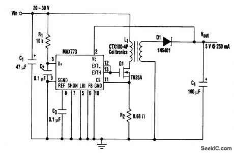
Adding a transformer to a step-up dc-to-dc regulator allows inputs of 20 V and higher to be accepted while operating in a step-down mode. The circuit handles inputs to 30 V, but is easily modifiable for high specific voltages. The transformer's 1:1 turns ratio simplifiers procurement by allowing the use of a standard, product (here, the Coiltronics CTX100-4P). Its 1:1 ratio also enhances stability by producing a duty cycle well below 50 percent. An ideal 1 : 1 transformer would generate Vin + Vout at the bottom of the primary, but real transformers produce somewhat higher voltages. That voltage appears across Q1, so Q1's minimum breakdown voltage should be approximately 2Vin +Vout. R2 limits the peak current (through Q1 and L1) to 0.33 A. The internal shunt regulator is a zener diode that is biased by R1 at approximately 2 mA. To cope with a wide range of input voltages, R1 can be replaced with a constant-current source. (View)
View full Circuit Diagram | Comments | Reading(1049)
| Pages:90/291 At 2081828384858687888990919293949596979899100Under 20 |
Circuit Categories
power supply circuit
Amplifier Circuit
Basic Circuit
LED and Light Circuit
Sensor Circuit
Signal Processing
Electrical Equipment Circuit
Control Circuit
Remote Control Circuit
A/D-D/A Converter Circuit
Audio Circuit
Measuring and Test Circuit
Communication Circuit
Computer-Related Circuit
555 Circuit
Automotive Circuit
Repairing Circuit