
Switching-Regulator Circuit
Index 5
Separately excited switching power supply circuit diagram using single-junction transistor as pulse generator
Published:2011/4/27 9:06:00 Author:Nicole | Keyword: switching power supply, single-junction transistor, pulse generator
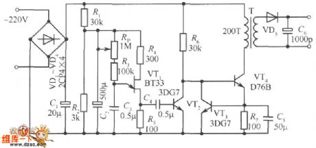
In figure: VD1 ~ VD4 and C1 is rectifying filter circuit, turning 220V AC network voltage into 300V DC voltage. Pulse generator consists of an unijunction transistor VT1, resistors R3, R4, R5, potentiometer RP and capacitor C3, to change the potentiometer's resistance can lead to the changing of pulse frequency. C4 is the coupling capacitor of output pulse. Rl and R2 divide 300V DC voltage to unijunction transistor VT1 and provide 20 ~ 30V operating voltage. VT2 is the inversion amplifier tube, it can invert and amplify the positive pulse outputed by pulse generator, transporting a negative pulse to switch VT4, so that it is ended when VT1 outputs positive pulse. (View)
View full Circuit Diagram | Comments | Reading(3342)
Pulse width modulated switching power supply circuit with stabilized voltage
Published:2011/4/27 9:05:00 Author:Nicole | Keyword: switching power supply, pulse width modulated
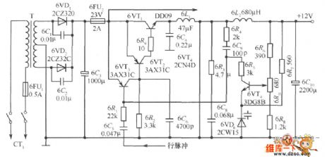
As shown, the main technical indicators are as follows: Output voltage: 12V; Output Current: 1A; power consumption <20W; efficiency> 64%; internal resistance <0.075Ω; ripple <15mV; mains voltage: 160 ~ 240V. Inthe figure, full-wave rectifier circuit is composed of 6VDl, 6VD2; 6C3 is the filter capacitor; 6C1, 6C2 areused to undermine the surge current; self-excited multivibrator is composed of 6VT1, 6VT2, 6VT3 and 6R4, 6C9, and the 6VT1 also is the switching tube. When the 12V output voltage decreases for some reason, the base of the error amplification 6VT4 obtained the voltage from the sampling circuit 6R6, 6R11, 6R8 also will be dropped, the collector voltage of 6VT4 rose, the potential base of 6VT3 also increased, the output pulse of the switch adjustment 6VT1 broadened, then the reduced voltage rising again. On the contrary, when the output voltage drops, it will make a reverse adjustment according to the aboveprocess, then keeping the output voltage steady.
(View)
View full Circuit Diagram | Comments | Reading(2483)
SANYO 83P Switching Power Supply Circuit
Published:2011/5/3 6:56:00 Author:Felicity | Keyword: SANYO Switching Power Supply Circuit,

The picture above shows the SANYO 83P Switching Power Supply Circuit. (View)
View full Circuit Diagram | Comments | Reading(1316)
SANYO 80P Switching Power Supply Circuit
Published:2011/5/3 6:44:00 Author:Felicity | Keyword: SANYO Switching Power Supply Circuit,
The picture above shows the SANYO 80P Switching Power Supply Circuit. (View)
View full Circuit Diagram | Comments | Reading(1644)
Hitachi Circuit of NP8C Switching Power
Published:2011/5/3 6:33:00 Author:Felicity | Keyword: Hitachi Circuit of Switching Power,
The picture above shows the Hitachi Circuit of NP8C Switching Power. (View)
View full Circuit Diagram | Comments | Reading(895)
Hitachi A1PM8C Switching Power Supply Circuit
Published:2011/5/3 6:27:00 Author:Felicity | Keyword: Hitachi Switching Power Supply Circuit,
The picture above shows the Hitchi A1PM8C Swotching Power Supply Circuit. (View)
View full Circuit Diagram | Comments | Reading(936)
TDA two chips switching power supply circuit diagram
Published:2011/4/28 9:31:00 Author:Rebekka | Keyword: two chips , switching power supply
TDA two chips switching power supply circuit diagram is shown as above. (View)
View full Circuit Diagram | Comments | Reading(4074)
Changing the output voltage of ringing switching power supply circuit diagram
Published:2011/4/22 18:45:00 Author:Nicole | Keyword: switching power supply
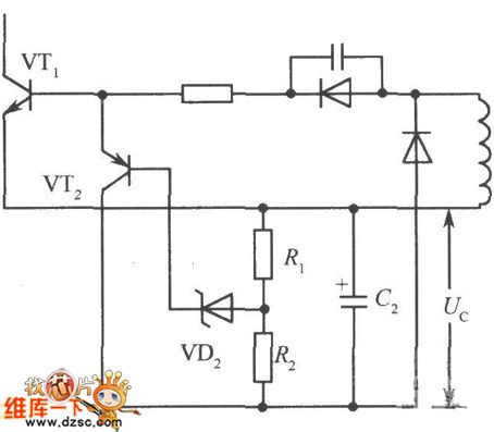
In the ringing choke type switching regulator circuit, the output voltage Uo is in direct proportion to the negative bias Uc, in order to change the output voltage, we should find a way to change Uc, as shown below.
The collector of transistor VT2 is connected on the negative terminal of capacitor C2. Once Uc2 increased, the base current of Zener diode VD2, transistor VT2 also increase, so that VT2 conducting. Because of the collector current VT2 can shorten the conduction time of switching transistor VTl than before, so it can be ended early, then to bring down the output voltage Uo.
(View)
View full Circuit Diagram | Comments | Reading(983)
Using KD-28 as voice switching circuit diagram
Published:2011/4/26 3:30:00 Author:Rebekka | Keyword: voice switching
Using KD-28 as voice switching circuit diagram is shown as above. (View)
View full Circuit Diagram | Comments | Reading(789)
Multi-Control Two Switch Circuit
Published:2011/4/21 20:18:00 Author:Robert | Keyword: Multi-Control, Two Switch Circuit
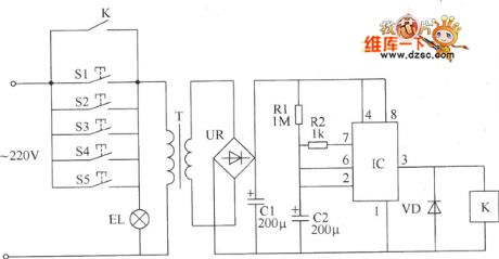
Multi-Control Two Switch Circuit is shown below:
(View)
View full Circuit Diagram | Comments | Reading(721)
Multi-Control Four Switch Circuit
Published:2011/4/21 20:19:00 Author:Robert | Keyword: Multi-Control, Four Switch
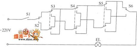
Multi-ControlFour Switch Circuit is shown below:
(View)
View full Circuit Diagram | Comments | Reading(711)
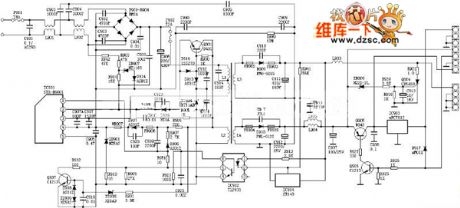
Hisense TC2102GD TV switching power supply (MC44608P75) circuit diagram
Published:2011/4/20 9:06:00 Author:Nicole | Keyword: Hisense, TV Power Supply
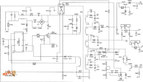
View full Circuit Diagram | Comments | Reading(3456)
Hisense ITV2911 TV switching power supply (KA3S0680R) circuit diagram
Published:2011/4/20 9:06:00 Author:Nicole | Keyword: Hisense, TV Power Supply
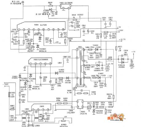
View full Circuit Diagram | Comments | Reading(4012)
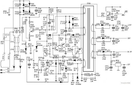
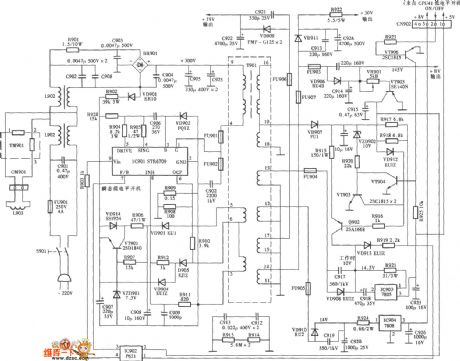
Based on staple Changhong PF2991E Large-screen flat screen color TV switching power supply circuit diagram
Published:2011/4/20 9:07:00 Author:Nicole | Keyword: Changhong, TV Power Supply

View full Circuit Diagram | Comments | Reading(3405)
Konka P2592N Mirror TV switching power supply (DTR-S6709A) circuit diagram
Published:2011/4/20 9:06:00 Author:Nicole | Keyword: Konka, TV Power Supply
View full Circuit Diagram | Comments | Reading(3169)
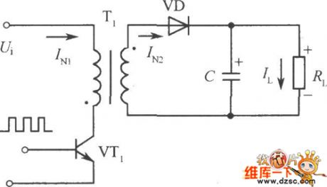
Single-ended flyback switching power supply circuit diagram
Published:2011/4/1 3:50:00 Author:Nicole | Keyword: single-ended switching power supply
View full Circuit Diagram | Comments | Reading(832)
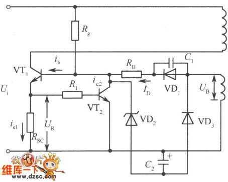
Protecting circuit diagram of ring switch on
Published:2011/4/1 3:51:00 Author:Nicole | Keyword: ring switch
View full Circuit Diagram | Comments | Reading(773)
MAX639 series multi-function integrated switching regulator circuit diagram of fixed / adjustable output
Published:2011/4/1 3:58:00 Author:Nicole | Keyword: integrated switching regulator
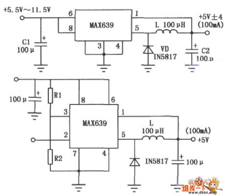
MAX639 series fixed / adjustable output multi-function integrated switching regulator circuit is an efficient, multi-function switching regulator circuit, the output voltage is +5 v, the input voltage is 5.5 ~ 11.5V, output current is 100mA. It is efficient, the electronic switch control terminal of the logic level control and the battery-side low-voltage detectionare havethe advantages of low-power, low dropout, multi-functional, it is widely used in portable instruments, meters and so on. The basic application as shown. The typical application circuit of voltage detection can be see as below.
(View)
View full Circuit Diagram | Comments | Reading(1852)
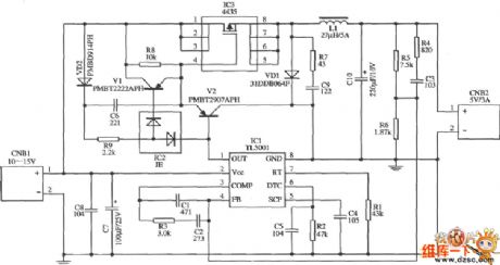
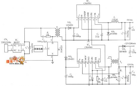
Application circuit diagram of switching regulator with input l0 ~ 15V / Output 5V/3A
Published:2011/4/1 3:32:00 Author:Nicole | Keyword: switching regulator
View full Circuit Diagram | Comments | Reading(1009)
Fore input power supply circuit diagram using depressurization switching power supply
Published:2011/4/20 9:05:00 Author:Nicole | Keyword: switching power supply
View full Circuit Diagram | Comments | Reading(993)
| Pages:5/8 12345678 |
Circuit Categories
power supply circuit
Amplifier Circuit
Basic Circuit
LED and Light Circuit
Sensor Circuit
Signal Processing
Electrical Equipment Circuit
Control Circuit
Remote Control Circuit
A/D-D/A Converter Circuit
Audio Circuit
Measuring and Test Circuit
Communication Circuit
Computer-Related Circuit
555 Circuit
Automotive Circuit
Repairing Circuit