
Switching-Regulator Circuit
Index 6
Single-ended flyback integrated switching power supply circuit diagram
Published:2011/3/30 3:20:00 Author:Nicole | Keyword: integrated switching power supply, Single-ended flyback
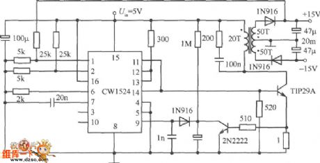
View full Circuit Diagram | Comments | Reading(832)
Boost switching regulator application circuit diagram
Published:2011/3/30 3:14:00 Author:Nicole | Keyword: switching regulator
View full Circuit Diagram | Comments | Reading(780)
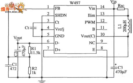
Output voltage polarity reversal application circuit diagram composed of components and W497
Published:2011/3/30 3:10:00 Author:Nicole | Keyword: Output voltage, component
View full Circuit Diagram | Comments | Reading(813)
Quasi-resonance switching power supply circuit diagram composed of WK212-166
Published:2011/4/12 4:04:00 Author:Nicole | Keyword: quasi-resonance, switching power supply
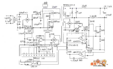
View full Circuit Diagram | Comments | Reading(1116)
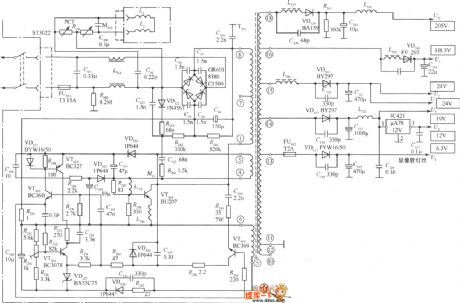
Color display switching power supply circuit diagram composed of STK7308
Published:2011/4/12 4:03:00 Author:Nicole | Keyword: color display, switching power supply
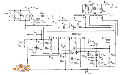
View full Circuit Diagram | Comments | Reading(2661)
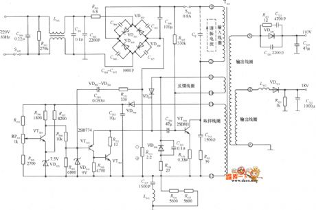
Switching power supply circuit diagram composed of STRS5941
Published:2011/4/12 4:03:00 Author:Nicole | Keyword: switching power supply
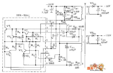
View full Circuit Diagram | Comments | Reading(2639)
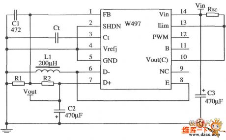
Buck switching regulator circuit diagram composed of W497
Published:2011/3/30 3:17:00 Author:Nicole | Keyword: switching regulator
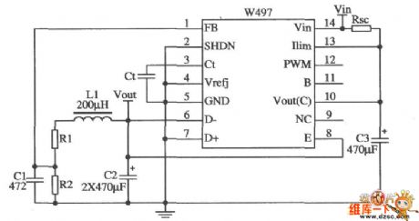
View full Circuit Diagram | Comments | Reading(785)
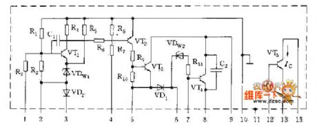
Separately excited switching power supply circuit diagram using self-excited multivibrator as pulse generator
Published:2011/4/1 3:56:00 Author:Nicole | Keyword: switching power supply, self-excited multivibrator, pulse generator
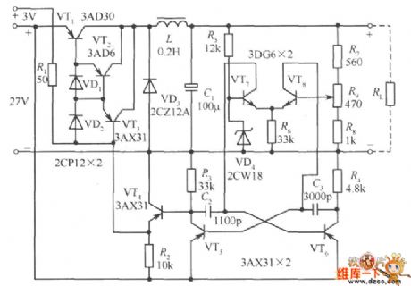
As shown, separately excited switching power supply circuit which used self-excited multivibrator as pulse generator, VTlis the switch tube; VT2, VT3are the push tubes; VT4is the emitter follower. Self-excited multivibrator as the separately excited oscillation circuit is composed of VT5, VT6, C2, C3, R3, R4 and so on. The emitter-coupled differential amplifier is made of VT7, VT8 which as the error amplification. Sampling circuit consists of resistors R7, R8 and R9 potentiometer in series. The reference voltage circuit composed of diode VD4 and R5. Diode VDl, VD2 is used to prevent the push tube VT2, VT3 emitter reversing voltage breakdown. VD3 for the after flow diode; L for the energy storage inductor. The turn-on and cut-off of switching regulator is flipped by the multivibrator, and controlled by emitter follower VT4. The time of multivibrator flip is determined by the error amplifier. The flip time of VT5 from the end to turn is determined by the charge current of VT8 to the C3. VT8 current is larger, the deadline of VT5 is longer. Similarly, The flip time of VT6 from the end to turn is determined by the charge current of VT7 to the C2 VT7 current is larger, the deadline of VL is shorter. When the output voltage down for some reason, VT8 tube collector current of the differential amplifier is decreased, VT7 tube collector current increases, so the conduction time of VT5 is shortened, extended the deadline, leading to the conduction time of VT4 longer, the deadline shorter, and ultimately the conduction time of control switch lengthened, shortened the deadline, so that the output voltage to rise, keep output voltage steady.
(View)
View full Circuit Diagram | Comments | Reading(1776)
Frequency modulated switching power supply circuit diagram with steady performance
Published:2011/4/1 3:55:00 Author:Nicole | Keyword: frequency modulated, switching power supply
As is shown in the figure, this is another example of switching power supply. The frequency changes are in range of 38 ~ 70kHz, when the input voltage changes are in range of 90 ~ 300V, it can maintain the stability of the output DC voltage.
(View)
View full Circuit Diagram | Comments | Reading(853)
Real-time high-voltage switching power supply circuit diagram
Published:2011/4/1 3:54:00 Author:Nicole | Keyword: Real-time, high-voltage, switching power supply
View full Circuit Diagram | Comments | Reading(1741)
Self-excited feedback transforming switching power supply circuit diagram
Published:2011/4/1 3:54:00 Author:Nicole | Keyword: switching power supply
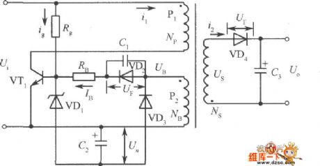
The basic principles of ringing choke-type as shown. When coupled with the input voltage, the current from Rg flowing to the base of switch VTl , so VTl conduction, when the diode of the transformer secondary side reverse biased, without current, so the streaming current of VT1 collector current and Np of transformer windings are equal. Because it is starting from zero, so the base current is not able to make VTl conduction. Rg is called the startup resistor.
(View)
View full Circuit Diagram | Comments | Reading(2494)
With zero current transition soft-switching power supply circuit diagram
Published:2011/4/1 3:48:00 Author:Nicole | Keyword: soft-switching power supply
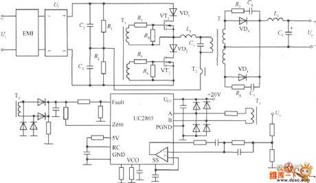
The figure of a zero current transition soft-switching power supply practical circuit as below: single-phase AC input; output DC; main switchadopts MOSFET; power converteradopts half bridge circuit; integrated control chipadopts UC2865; power conversion adopts zero current transformation circuit.
(View)
View full Circuit Diagram | Comments | Reading(2587)
5V/2A isolated switching power supply circuit diagram
Published:2011/4/6 3:15:00 Author:Nicole | Keyword: switching power supply, isolated
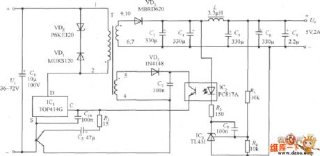
The circuit diagram as shown. C1 stands for the input filter capacitor. VDz and VD1 formonce sideclamp protection circuit. R1 is the resistance of the controlled end, C2 is a bypass capacitor. C10 is paralleled between TOP414GC-S-side to prevent high frequency interference occurring in the control side and caused power circuit malfunction. VD2 represents the output rectifier diodes, C3, C4, L, C5 and C6 form the output filter, C9 for the output Noise capacitor. External error amplifier is composed of the shunt regulator TL431. When the output voltage fluctuations, the samples obtained after R3, R4 partial pressure, compared with TL431 voltage reference, resulting in an external control signal, and then through the optical coupler PC817A to change TOP414G control terminal current, thereby regulating the track duty stabilize the Uo. Control loop gain is set by the R2. After VD3, C7 rectifier filter, the feedback winding voltage give the infrared receiver of PC817A power supply.
(View)
View full Circuit Diagram | Comments | Reading(6456)
Pocket switching power supply charger circuit diagram
Published:2011/4/1 3:39:00 Author:Nicole | Keyword: charger, switching power supply
View full Circuit Diagram | Comments | Reading(1644)
IX0308CE series switching power supply thick film circuit diagram
Published:2011/4/11 4:13:00 Author:Nicole | Keyword: switching power supply
View full Circuit Diagram | Comments | Reading(752)
IX0247CE series switching power supply thick film circuit diagram
Published:2011/4/11 4:13:00 Author:Nicole | Keyword: switching power supply
View full Circuit Diagram | Comments | Reading(658)
IX0689CE series switching power supply thick film circuit diagram
Published:2011/4/11 4:13:00 Author:Nicole | Keyword: switching power supply
View full Circuit Diagram | Comments | Reading(744)
STR440 series switching power supply thick film circuit diagram
Published:2011/4/11 4:13:00 Author:Nicole | Keyword: switching power supply
View full Circuit Diagram | Comments | Reading(1120)
STR5312 series switching power supply thick film circuit diagram
Published:2011/4/11 4:12:00 Author:Nicole | Keyword: switching power supply
View full Circuit Diagram | Comments | Reading(780)
STR6020 series switching power supply thick film circuit diagram
Published:2011/4/11 4:12:00 Author:Nicole | Keyword: switching power supply
View full Circuit Diagram | Comments | Reading(958)
| Pages:6/8 12345678 |
Circuit Categories
power supply circuit
Amplifier Circuit
Basic Circuit
LED and Light Circuit
Sensor Circuit
Signal Processing
Electrical Equipment Circuit
Control Circuit
Remote Control Circuit
A/D-D/A Converter Circuit
Audio Circuit
Measuring and Test Circuit
Communication Circuit
Computer-Related Circuit
555 Circuit
Automotive Circuit
Repairing Circuit