
Switching-Regulator Circuit
Index 4
STR-F6656 switching power supply thick film integrated circuit
Published:2011/6/15 7:32:00 Author:chopper | Keyword: switching power supply, thick film
STRF6656 is a mixed type switching power supply thick film integrated circuit (View)
View full Circuit Diagram | Comments | Reading(1929)
STR-F6654 switching power supply thick film integrated circuits
Published:2011/6/15 7:33:00 Author:chopper | Keyword: switching power supply, thick film
STRF6654 is a kind of mixed type switching power supply thick film integrated (View)
View full Circuit Diagram | Comments | Reading(1597)
Switch D. C. Regulated Power Supply Two
Published:2011/6/3 4:39:00 Author:Michel | Keyword: Switch, D. C., Regulated Power Supply, Two
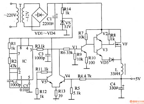
This example introduces the switch D. C. regulated power supply circuit of buck-mode +5V series.It is composed of power supply circuit,impulsator,voltage sampling or pulse width modulation circuit, buffering driver circuit and it is showed as the picture 5-38.The input converting circuit consists of mains transformer,T,commutation diode VD1-VD4,filter capacitor C1,current-limiting resistor and voltage regulator diode VS.The impulsator consists of time-base integrated circuit IC,resistor,R1,R2 and capacitor,C2,C5.The voltage sampling or pulse width modulation circuit is composed of capacitor,C3,resistor,R3-R5,R11-R13 and transistor V4 and V5. (View)
View full Circuit Diagram | Comments | Reading(2852)
Switch D. C. Regulated Power Supply One
Published:2011/6/3 3:52:00 Author:Michel | Keyword: Switch , D. C., Regulated Power Supply, One
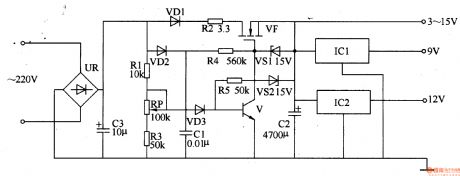
The switch D. C. regulated power supply circuit introduced in the example can supply 3-15V D.C. voltage and its maximum current is 150mA,which meet the miniaturized electronics' power supply.
Work's Principle of the CircuitThe switch D. C. regulated power supply circuit is composed of rectifying and wave-filtering circuit,switch control circuit and voltage regulator circuit and it is showed as the picture 5-37.
The rectifying and wave-filtering bridge,UR,commutation diode,VD1,VD2 and filter capacitor,C1 and C3.The switch control circuit consists of resistor,R2 and R4,voltage regulator diode,VS1 and field effect transistor,VF.The voltage regulator circuit is composed of resistor R1,R3,R5,voltage regulator diode VS2,transistor,V,diode,VD3,filter capacitor C2 and three-terminal integrated regulator IC1 and IC2.
(View)
View full Circuit Diagram | Comments | Reading(1216)
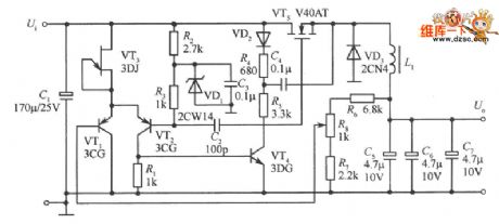
switching-regulator circuit reformed by waste energy-saving lamp
Published:2011/5/24 23:45:00 Author:Ariel Wang | Keyword: switching-regulator circuit, waste, evergy-saving lamp
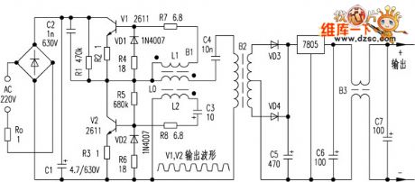
When it isbeingused,it's not proper to take voltage from C5 directly. It's imposible to allow short circuit happened, otherwise it'll burn V1 and V2. Because when short circuit takes place,the electric currentin coil LO of flyback transformer B1 will increase rappidly.The voltage of coil L1 and L2 increases to a rather high level.It gives back the electric currentin V1 and V2 increasing as well. It causes intensive positive feedback.Finally it burns out as the limitation of power consumption of V1 and V2. This feedback of circuit belongs to series circuit feedback.And it can openand protectcircuit. But when load is increased,the feedback is strenghened.What's more,the frequency will decrease as the load increases. The internal resistance is rather small,so short circuit will burn pliotron very easily.
(View)
View full Circuit Diagram | Comments | Reading(1031)
Switching power supply of artificial circuit diagram
Published:2011/6/2 21:45:00 Author:Sophia | Keyword: Artificial circuit, Switching power supply
(View)
View full Circuit Diagram | Comments | Reading(819)
Switch D. C. Regulated Power Supply Three
Published:2011/6/3 5:00:00 Author:Michel | Keyword: Switch, D. C., Regulated Power Supply, Three
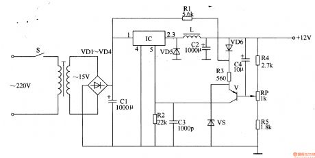

The switch D. C. regulated power supply circuit introduced in the example uses TWH8778 electronic switching IC and it has high work's efficiency,its circuit is simple which is easy to manufature.The output voltage and current of the power supply circuit are +12V and 1A respectively.
Work's Principle of the CircuitThe switch D. C. regulated power supply circuit is composed of input converting circuit,switch output circuit and automatical voltage regulator circuit and it is showed as the picture 5-39.
The input converting circuit consists of mains switch S,mains transformer T,commutation diode VD1-VD4 and filter capacitor C1.The switch output circuit is composed of electronic switching intergrated circuit,IC,resistor R1,R2, diode,VD5,induction coil,L and capacitor C2,C3. (View)
View full Circuit Diagram | Comments | Reading(1220)
switching power supply constant current charger circuit
Published:2011/6/4 13:13:00 Author:John | Keyword: constant current charger
Switching power supply constant current charger circuit is shown below.
(View)
View full Circuit Diagram | Comments | Reading(4653)
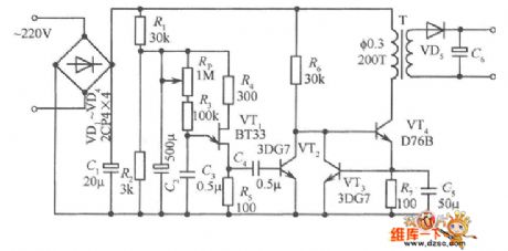
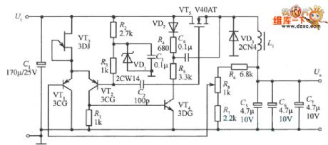
one switching-regulator circuit
Published:2011/6/4 13:28:00 Author:John | Keyword: switching-regulator
One switching-regulator circuit is shown in the following.
(View)
View full Circuit Diagram | Comments | Reading(1627)
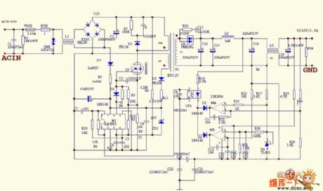
LWT2005 type ATX switch power supply circuit diagram
Published:2011/5/11 2:48:00 Author:Rebekka | Keyword: switch power supply

Here is the diagram of LWT2005 type ATX switch power supply circuit.
(View)
View full Circuit Diagram | Comments | Reading(12301)
200W ATX switching power supply circuit diagram
Published:2011/5/11 2:43:00 Author:Rebekka | Keyword: switching power supply
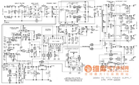
Here is the diagram of 200W ATX switching power supply circuit. (View)
View full Circuit Diagram | Comments | Reading(4554)
Application circuit diagram of simplified VMOS switching power supply
Published:2011/5/5 7:27:00 Author:Nicole | Keyword: switching power supply, VMOS
VMOS switching power supply circuit diagram. Because of adopting voltage comparator 710, so the circuit issimpler than former. As shown, resistor R1, R2, R3 and regulator VDl, VD2 form divider regulator circuit, three groups of 5V, 6V and 18V are separated from 28V input voltage,they areused as the power supply; resistors R12, R13, capacitor C13, diodes VD6, VD7 and transistor VT3 constitute the power soft-start circuit. The moment of power turn on, the drive pulse width of VMOS tube VTl increases exponentially. when the comparator 710 cut off the drive pulse firstly, it can prevent the current of energy storage inductor too large. When the switch VTl cut down, the output voltage of switching power supply continues to rise because the current of energy storage inductor L1 still charge to the output filter capacitor C6 ~ C12. In other words, soft-start circuit make the current of energy storage inductor L1 rise slowly when the power supply start working, then to prevent output voltage from large overshoot. After the power supply into steady-state, the soft-start circuit is not work.
(View)
View full Circuit Diagram | Comments | Reading(1395)
Separate excitation switching power supply circuit diagram using free-running multivibrator as pulse generator
Published:2011/5/5 7:32:00 Author:Nicole | Keyword: switching power supply, multivibrator, pulse generator
As shown, VTlis the switch; VT2, VT3is push tube; VT4 is emitter follower. Separate excitation oscillation circuit is undertaken by free-running multivibrator which composed of VT5, VT6, C2, C3, R3, R4. VT7, VT8 form emitter-coupled differential amplifier to be used as the error amplification. Sampling circuit consists of resistors R7, R8 and in series with potentiometer R9. Voltage reference circuit is made of regulator diode VD4 and R5. Diode VDl, VD2 is used to prevent reverse voltage breakdown the push tube VT2, VT3 emitter. VD3 for the freewheeling diode; L for the energy storage inductor.
The turn on/off of switch regulator is flipped by multivibrator, and controlled by emitter follower VT4. The flip time of multivibratoris determined by the error amplifier. In other words, The flip time of VT5 from the end to turnare decided by the current of VT8 charge to C3. The current of VT8 is larger, the deadline of VT5 is longer. Similarly, the flip time of VT6 from the end to turn is decided by the current of VT7 charge to C2. The current of VT7 is larger, the deadline of VT5 is shorter. When the output voltage isdropped for some reason, VT8 tube collector current of the differential amplifier decreases, tube collector current of VT7increases, so the conduction time of VT5 is shortened, and extended the deadline, leading to the longerconduction time of VT4 longer, the cut-off shorter, and ultimately the conduction time of control switch tubeis lengthening, the deadline is shortening,so that the output voltage to rise, remain the stability of output voltage.
(View)
View full Circuit Diagram | Comments | Reading(1680)
Jinxing C7458 Switching Power Supply Circuit
Published:2011/5/5 9:48:00 Author:Felicity | Keyword: Switching Power Supply Circuit,
The picture above shows Jinxing C7458 Switching Power Supply Circuit. (View)
View full Circuit Diagram | Comments | Reading(1083)
Separate-excited Single-ended Flyback Switching Power Supply 4C7108 Circuit
Published:2011/5/5 9:49:00 Author:Felicity | Keyword: Separate-excited Single-ended Flyback Switching Power Supply Circuit,
The picture above shows the stimulated single-ended flyback switching power supply 4C7108 circuit. (View)
View full Circuit Diagram | Comments | Reading(1234)
Panasonic M12H Switching Power Supply Circuit
Published:2011/5/5 9:52:00 Author:Felicity | Keyword: Panasonic, Switching Power Supply Circuit,
The picture above shows the Panasonic M12H Switching Power Supply Circuit. (View)
View full Circuit Diagram | Comments | Reading(1058)
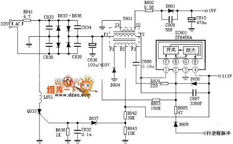
Based on a pulse regulating neon type switching regulated power supply circuit diagram
Published:2011/4/22 18:53:00 Author:Nicole | Keyword: switching power supply
This is a pulse Ni switching power supply circuit diagram, it is Kaige 4D17U produced by radio four factory in Shanghai. The power supply of 35cm black and white TV.
The main technical indicators are as follows: Output voltage: 12V; Output Current: 1A; power consumption <20W; efficiency> 64%; resistance <0.075Ω; ripple <15mV; mains voltage: 160 ~ 240V.
As shown, 6VDl, 6VD2 form full-wave rectifier circuit; 6C3is filter capacitor; 6C1, 6C2 are used to weaken the inrush current; 6VT7, 6VT2, 6VT3 and 6R4, 6C9 constitute the self-excited multivibrator, 6VT7 also is the switching tube.
When the 12V output voltage decreases for some reason, the base of error amplification 6VT5 obtain the voltage from the sampling circuit 6R6, 6R9, 6R8 also drop, the collector voltage of 6VT5 rises, potential base 6VT3 increases, the output pulse of switch controls tube 6VT7 widen, then the reducing voltage rises again. On the contrary, to adjust on the opposite by the above process when the output voltage goes down, to make the output voltage stable.
(View)
View full Circuit Diagram | Comments | Reading(2089)
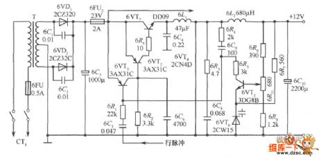
Strong stability boost output circuit diagram
Published:2011/4/7 3:44:00 Author:Nicole | Keyword: boost, output
The figure is a boost output type practical circuit. VT3 is the switching regulator; regulator VD2 can change the potential; VT4 is inverting isolation amplifier; Ui is divided by the VT4 and its 33kΩ load resistor. The two voltage supply for pulse generator circuit. Pulse generator circuit consists of the transformer T and VTl, VT2. This is a non-symmetric transformer feedback self-excited multivibrator. The supply of VTl is from the voltage of 33kΩ load resistor, and the current of resistance depends on the current of VT4. VT1, VT2 have different supply voltage, the oscillation amplitude of half and half weeks is changed in direct proportion, the width is inversely proportional to the change, to control the on and off time of VT3. When the output voltage increases, the differential pair VT6 current of error amplifier increases, VT5 current decreases, the collector potential rise, VT4 current increases, 33kΩ resistor voltage drop increases, VTl pipe supply pressure is increased, conduction time is shortened, the conduction time of switch VT3 is shortened, too.
The circuit input voltage is 12 ~ 28V, the output can be stable for 30V, maximum output power is 60W, efficiency is 89.4% ~ 94.7%, instability is ± 0.33%, the ripple coefficient of output voltage is 0.02%, operating frequency is 10kHz.
(View)
View full Circuit Diagram | Comments | Reading(947)
Ring-type switching power supply constant current drive circuit diagram
Published:2011/3/30 3:29:00 Author:Nicole | Keyword: switching power supply, constant current drive
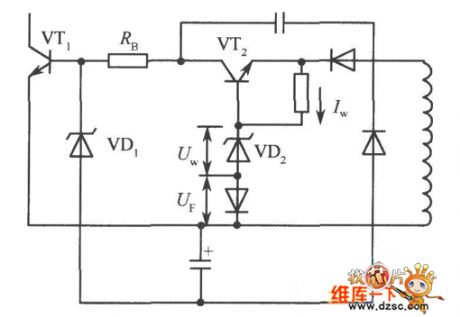
It is essentially a simple series regulator. The load is a fixed resistor RB. Even if the input voltage Ui changes, the current flowing through RB is constant. This will not only significantly reduce the loss of the resistance, but also to prevent intermittent oscillation. AC is in range of 100 ~ 200V, the power can work continuously.
In the ring-type switching power supply, the loss of the drive circuit of supply switching transistor base current is considerable. In addition to ensuring the switching transistor can fully turn with the minimum input voltage, the voltage UB on the transformer winding is in direct proportion to the input voltage Ui. when Ui rises, the drive current Id increases too, and the incremental losses of the base resistance Rb, can increase with the square of increasing part of Id.
When the drive current ID is increasing, the current of the branch of regulator diode must be increased, it may cause oscillation, that is, the switching works in a period of time, but will stop working in the adjacent time. Over and over again, the frequency of oscillation is about several hundred to several thousand Hertz.
To solve these problems, that is, when the input voltage changes, it can adopt constant current drive to remain drive current unchanged, as shown below.
(View)
View full Circuit Diagram | Comments | Reading(999)
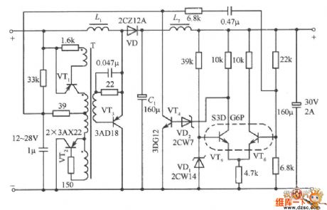
Regulated power supply circuit diagram used VMOS as switching element
Published:2011/4/8 2:38:00 Author:Nicole | Keyword: regulated power supply, switching element
As shown, it is a power supply circuit used VMOS as switching element. VT5 is VMOS power transistor, the switch adjustment element of power supply; L1is the energy storage inductor; VD3 for the freewheeling diode; VT3 for the FET, as the constant current source of VTl, VT2, to provide the emitter with lmA constant current; Cl is the input filter capacitor; C5, C6, C7 is the output filter capacitor.
It is determined by the relative voltage of the two base to turn on VTl or VT2 first. If the base potential of VT1 below VT2, the VTl on, VT2 off; on the contrary, the VTl off, VT2 on. The base potential of VT2 is decided by resistances R2, R3 and voltage regulator diode VD1, it is a constant; and base potential of VTl is obtained from the output voltage through the resistor R6C R, and derived from the potentiometer R8, the output voltage can be changed by adjusting potentiometer R8.
In order to reduce the power consumption of switch regulator VT5, to improve its turning speed, the circuit adopts bootstrap network which composed of R5, C4. When VT5 is off, the source potential is 0V, the input voltage charge to C4 through diode VD2 resistor R4, so that the voltage on C4 is close to the input voltage. When VT5 is on, the source potential rise, as there is sufficient voltage on the capacitor C4, so that the diode VD2 off, by this time, the voltage on R5 is close to 2 times the input voltage, so VT5 turn on more quickly. At this point even if the input voltage is low, the circuit also can be flipped. The role of C2, C3 is to make VT1, VT2 flip quickly, then to improve the speed of switching.
(View)
View full Circuit Diagram | Comments | Reading(1444)
| Pages:4/8 12345678 |
Circuit Categories
power supply circuit
Amplifier Circuit
Basic Circuit
LED and Light Circuit
Sensor Circuit
Signal Processing
Electrical Equipment Circuit
Control Circuit
Remote Control Circuit
A/D-D/A Converter Circuit
Audio Circuit
Measuring and Test Circuit
Communication Circuit
Computer-Related Circuit
555 Circuit
Automotive Circuit
Repairing Circuit