Want to post a buying lead? If you are not a member yet, please select the specific/related part number first and then fill the quantity and your contact details in the "Request for Quotation Form" on the left, and then click "Send RFQ".Your buying lead can then be posted, and the reliable suppliers will quote via our online message system or other channels soon.
The FDmesh™ associates all advantages of reduced on-resistance and fast switching with an intrinsic fast-recovery body diode. It is therefore strongly recommended for bridge topologies, in particular ZVS phase-shift converters.
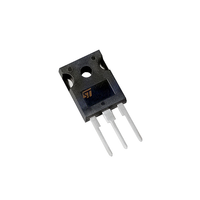
STW45NM50FD Maximum Ratings
Symbol
Parameter
Value
Unit
VDS
Drain-source Voltage (VGS = 0)
500
V
VDGR
Drain- gate Voltage (RGS = 20 k)
500
V
VGS
Gate-Source Voltage
± 30
V
ID
Drain Current (continuous) at Tc = 25
45
A
ID
Drain Current (continuous) at Tc = 100
28.4
A
IDM(`)
Drain Current (pulsed)
180
A
PTOT
Total Dissipation at Tc = 25
417
W
Derating Factor
2.08
W/
dv/dt(1)
Peak Diode Recovery voltage slope
20
V/ns
Tstg
Storage Temperature
65 to 150
Tj
Max. Operating Junction Temperature
150
(`) Pulse width limited by safe operating area (1) ISD 45A, di/dt400A/µs, VDD V(BR)DSS, Tj TJMAX.
STW45NM50FD Typical Application
ZVS PHASE-SHIFT FULL BRIDGE CONVERTERS FOR SMPS AND WELDING EQUIPMENT
The MDmesh™ is a new revolutionary MOSFET technology that associates the Multiple Drain process with the Company's PowerMESH™ horizontal layout. The resulting product has an outstanding low on-resistance, impressively high dv/dt and excellent avalanche characteristics. The adoption of the Company's proprietary strip technique yields overall dynamic performance that is significantly better than that of similar competition's products.
STW45NM60 Maximum Ratings
Symbol
Parameter
Value
Unit
VDS
Drain-source Voltage (VGS = 0)
600
V
VDGR
Drain- gate Voltage (RGS = 20 k)
600
V
VGS
Gate-source Voltage
±30
V
ID
Drain Current (continuous) at Tc = 25
45
A
ID
Drain Current (continuous) at Tc = 100
28
A
IDM(•)
Drain Current (pulsed)
180
A
PTOT
Total Dissipation at Tc = 25
417
W
Derating Factor
3.33
W/
dv/dt(1)
Peak Diode Recovery voltage slope
15
V/ns
Tstg
Storage Temperature
-65 to 150
Tj
Max. Operating Junction Temperature
150
(•)Pulse width limited by safe operating area (1)ISD 45A, di/dt 400A/µs, VDD V(BR)DSS, Tj TJMAX.
STW45NM60 Typical Application
The MDmesh™ family is very suitable for increasing power density of high voltage converters allowing system miniaturization and higher efficiencies.
STW47NM50 General Description
The MDmesh™ is a new revolutionary MOSFET technology that associates the Multiple Drain process with the Company's PowerMESH™ horizontal layout. The resulting product has an outstanding low on-resistance, impressively high dv/dt and excellent avalanche characteristics. The adoption of the Company's proprietary strip technique yields overall dynamic performance that is significantly better than that of similar competition's products.
STW47NM50 Maximum Ratings
Symbol
Parameter
Value
Unit
VDS
Drain-source Voltage (VGS = 0)
500
V
VDGR
Drain- gate Voltage (RGS = 20 k)
500
V
VGS
Gate-source Voltage
±30
V
ID
Drain Current (continuous) at Tc = 25
45
A
ID
Drain Current (continuous) at Tc = 100
28.4
A
IDM(•)
Drain Current (pulsed)
180
A
PTOT
Total Dissipation at Tc = 25
417
W
Derating Factor
2.08
W/
dv/dt(1)
Peak Diode Recovery voltage slope
15
V/ns
Tstg
Storage Temperature
-65 to 150
Tj
Max. Operating Junction Temperature
150
(•)Pulse width limited by safe operating area (1)ISD 45A, di/dt 400A/µs, VDD V(BR)DSS, Tj TJMAX.
STW47NM50 Typical Application
The MDmesh™ family is very suitable for increasing power density of high voltage converters allowing system miniaturization and higher efficiencies.