
555 Circuit
Index 41
555 voltage detection circuit
Published:2011/4/27 3:41:00 Author:Ecco | Keyword: 555, voltage detection
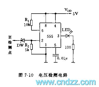
As shown in Figure 7-10, the voltage detection circuit uses 555 as the core to form in bistable mode. Usually, the pin 6 of 555 (threshold level side)is connected to VDD by R1, therefore, pin 3 is in low level. The pin 2 on trigger end of 555 is connected to the measured point by a regulator DW, DW regulator is Vz, when the measured voltage is less than Vz +1/3 VDD, the 555 sets, pin 3 is high level, LED is lit. If using different value of regulators DW, it is controlled by the switch, you can distinguish the different values of the measured voltage.
(View)
View full Circuit Diagram | Comments | Reading(2230)
555 quickly resistance measuring circuit
Published:2011/4/27 3:32:00 Author:Ecco | Keyword: 555 , quickly , resistance, measuring
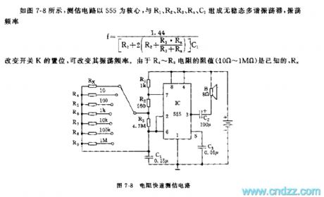
As shown in Figure 7-8, measuring circuit uses 555 as the core, and 555,R1, R2, R3, Rx, C1 form an astable multivibrator.
Changing the switch K can change the oscillation frequency. Since R4 ~ R9 resistor (10Ω ~ 1MΩ) is known, Rx is the resistance under test,it caneasily and quickly determine the resistance of Rx by the comparison of the sound with correspondingoscillation frequency of known resistors.
(View)
View full Circuit Diagram | Comments | Reading(855)
555 Optical toy car circuit
Published:2011/4/26 22:19:00 Author:Ecco | Keyword: 555, Optical , toy car
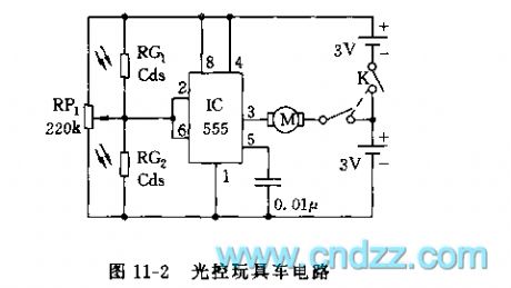
As shown in Figure 11-2, IC (555) is connected as dual stable trigger. RG1, RG2 are photoresistors, which are packed in the car's left window and right window (or front and back), when the RG1 is suffered illumination, its resistance declines sharply, pin 6 is in high level, 555 resets, pin 3 is in low level, the motor M reversing and turning right; or turning left. (View)
View full Circuit Diagram | Comments | Reading(997)
Toyota Coaster bus engine circuit diagram
Published:2011/4/27 2:15:00 Author:Rebekka | Keyword: Toyota Coaster , bus engine
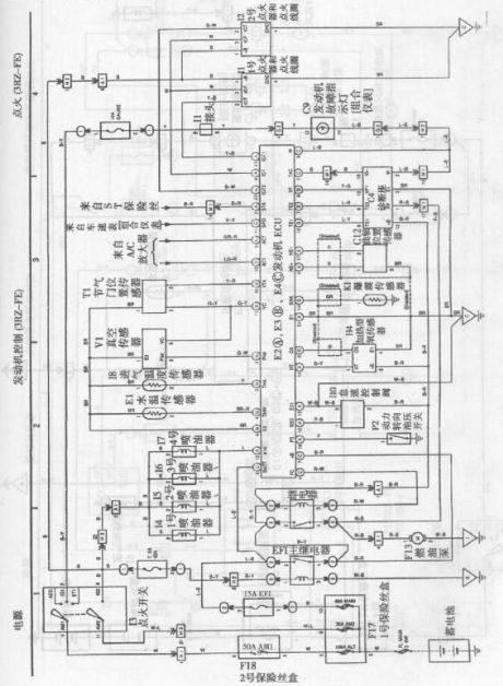
Toyota Coaster bus engine circuit diagram is shown as above. (View)
View full Circuit Diagram | Comments | Reading(3732)
555 Inductive switching power supply circuit
Published:2011/4/27 2:35:00 Author:Ecco | Keyword: 555 , Inductive , switching , power supply
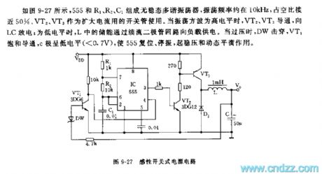
As shown in Figure 9-27, 555 and R1, R2, C1 form an astable multivibrator, the oscillation frequency is about 10kHz, duty cycle closes to 50%. VT2, VT3 are used as the switching tube to expand the current. When the shock wave is in high level, VT2, VT3 are conducted to discharge for LC ; when it is in low level, the energy storage in L provides power for load through the freewheeling diode loop. When overvoltage, DW is punctured, VT1 is saturated conducted, C is in low level, so that 555 resets and stops vibration, it plays the role of regulation and homeostasis.
(View)
View full Circuit Diagram | Comments | Reading(2494)
555 special power supply for razor
Published:2011/4/27 2:18:00 Author:Ecco | Keyword: 555 , special power supply , razor
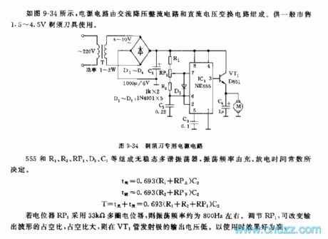
As shown in Figure 9-34, the power circuit is composed of AC step-down rectifier circuit and DC voltage conversion circuit. It is used for 1.5V ~ 4.5V razors sold in general market. 555 and R1, R2, RP1, D5, C2 etc. form an astable multivibrator, the oscillation frequency is decided by the charging and discharging time constant. If the potentiometer RP1 uses 33kΩ multi-turn potentiometer, the oscillation frequency is about 800HZ, adjusting RP1 can change the output waveform duty cycle, the duty cycle is large while the output voltage of the emitter of VT1 pipe is low. The using effect is the criterion.
(View)
View full Circuit Diagram | Comments | Reading(819)
Toyota Coaster bus automatic door circuit diagram
Published:2011/4/26 20:23:00 Author:Rebekka | Keyword: Toyota Coaster bus , automatic door
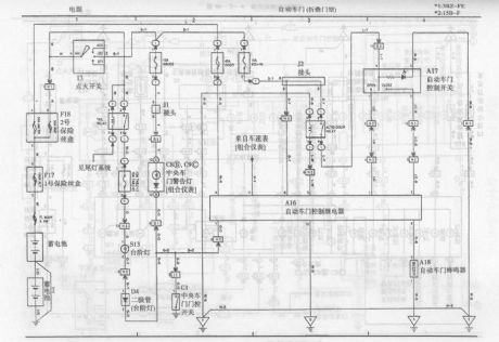
Toyota Coaster bus automatic door (folding doortype) circuit diagram (View)
View full Circuit Diagram | Comments | Reading(4911)
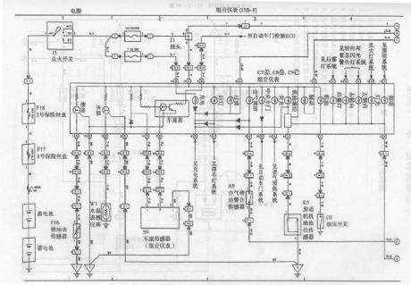
Toyota Coaster bus combination instrument circuit diagram 1
Published:2011/4/26 20:21:00 Author:Rebekka | Keyword: Toyota Coaster bus, combination instrument
View full Circuit Diagram | Comments | Reading(864)
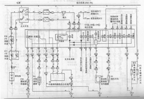
Toyota Coaster bus combination instrument circuit diagram 2
Published:2011/4/26 20:20:00 Author:Rebekka | Keyword: Toyota Coaster bus, combination instrument
Toyota Coaster bus combination instrument circuit diagram is shown as above. (View)
View full Circuit Diagram | Comments | Reading(1130)
Toyota Coaster bus combination instrument circuit diagram 3
Published:2011/4/26 20:02:00 Author:Rebekka | Keyword: Toyota Coaster bus , combination instrument
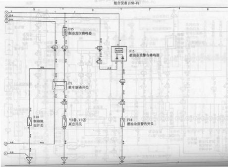
Toyota Coaster bus combination instrument circuit diagram is shown as above. (View)
View full Circuit Diagram | Comments | Reading(894)
555 Vco circuit with logarithmic characteristic
Published:2011/4/26 3:11:00 Author:Ecco | Keyword: 555 , Vco , logarithmic characteristic
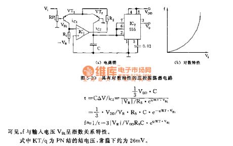
As shown in Figure 5-20, 555 and IC1, VT1, C etc. form VCO, the changing of input voltage VB1 causes the oscillation frequency of IC2 changing with logarithmic characteristics. VT1, VT2 are the same curve matching tube, because the base of VT2 is in zero potential, while VB1 changes, it can be equivalent to the VBE2 changing of VT2.
Capacitor charging current is the ic2, the relation between the input voltage VB1 and f has exponential characteristics. KT / q is the junction voltage of PN junction, it is about 26mV under room temperature.
(View)
View full Circuit Diagram | Comments | Reading(2219)
555 Gate Pulse Generator Circuit
Published:2011/4/26 8:28:00 Author:Robert | Keyword: Gate Pulse Generator
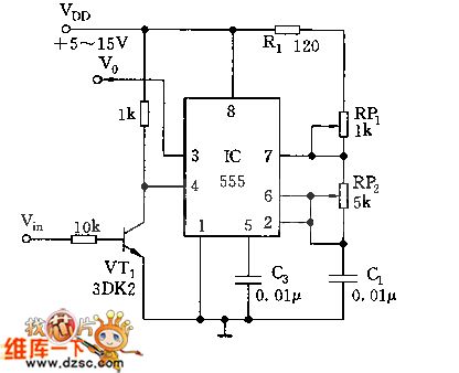
As shown, 555 and RP1, RP2, C1 compose the controllable multivibrator, its oscillation frequency depends on the constant time of R1, RP1, RP2, C1. But the oscillation depends on the voltage level of the input gate wave. When the Vln is high voltage level, VT1 is saturatedand conducted, the 4 foot of 555 is low voltage level,force the 555 resets, with no output; When the VlnO is low voltage level, VT1 closes, 555 is in a state of free oscillation, its 3 foot outputs the sequence oscillationsquare wave.
(View)
View full Circuit Diagram | Comments | Reading(2052)
555 Gauge Head Frequency Meter Circuit
Published:2011/4/26 7:47:00 Author:Robert | Keyword: Gauge Head, Frequency Meter
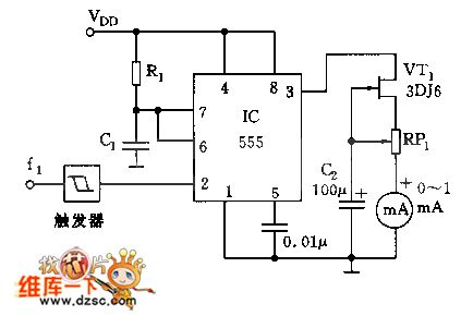
As shown, 555 and R1, C1 etc. compose a monostable delay circuit, input square wave signal or the square wave signal after the shaping of Schmitt trigger, trigger 555.The circuitrequires the time constant R1C1<Tin, Tin is the cycle time of input pulse signal. Or, input signal can not trigger 555 every time, and flip it.
VT1, RP1 areconstant current source, by adjusting RP1 make the mA meter to be full scaleata frequency. The relationship between the gauge head and frequency is: when the frequency become higher, as the duty cycle increases, the average current increases too, the pointer deflectionis larger; otherwise, the deflection is smaller.
(View)
View full Circuit Diagram | Comments | Reading(2149)
555 linear sawtooth wave generator circuit
Published:2011/4/26 2:50:00 Author:Ecco | Keyword: 555 , linear, sawtooth wave, generator
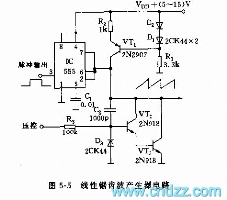
The circuit shown in Figure 5-5 is a sawtooth-wave circuit composed of the monostable trigger circuit, cross-flow circuit. VT1 and D1, D2, Rt form constant current charging circuit to make a good ramp linearity. The charging time constant of 555 monostable circuit is mainly decided by R2, C2. The circuit can produce linearity sawtooth in several HZ to 50kHz frequency range of broadband. This circuit can be used in a variable time base circuit, current - frequency converter and audio synthesizers and other occasions.
(View)
View full Circuit Diagram | Comments | Reading(4179)
555 darkroom timer circuit 1
Published:2011/4/26 3:23:00 Author:Ecco | Keyword: 555 , darkroom, timer
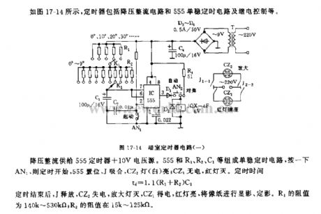
As shown in Figure 17-14, the timer includes buck rectifier circuit and 555 single stable control circuit and relay control. Buck rectifier provides +10 V voltage source for 555 timer. 555 and R1, R2, C1 form a single stable timing circuit, clicking the AN1, the timer starts, 555 sets, J pulls in, CZ2 is lit; CZ1 has no electricity, lights is off. Regular time td = 1.1 (R1 + R2) C1. After timing, J releases, CZ2 loses power, enlarger lamp gets power, the red lamp is lit, CZ1 gets electric, the red light will be like a paper developing and fixing. The resistance of R1 is 140K ~ 530kΩ; the resistance of R2 is 15k ~ 125kΩ.
(View)
View full Circuit Diagram | Comments | Reading(1780)
555 square wave generator circuit diagram
Published:2011/4/26 10:48:00 Author:Nancy | Keyword: square wave, generator
View full Circuit Diagram | Comments | Reading(1295)
555 simple and practical gust circuit
Published:2011/4/26 1:34:00 Author:Ecco | Keyword: 555 , simple , practical , gust circuit
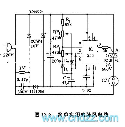
The circuit shown as the figure 12-8 consists of step-down rectifier and vibration control. The supply voltage VDD of IC (555) is about 10V. Because of the connection C, once getting power, 555 sets, SCR trigger is conducted, CZ has power, fan operates. When the threshold level of C is charged to be higher than 2/3, the 555 resets and fan stops. The stopping time of fan, that means t discharge = 0.693RP2C; fan operation time, t charge = 0.693 (R1 + RP1) C.
(View)
View full Circuit Diagram | Comments | Reading(2190)
555 imitating natural wind circuit 2
Published:2011/4/25 22:29:00 Author:Ecco | Keyword: 555 , imitating , natural wind
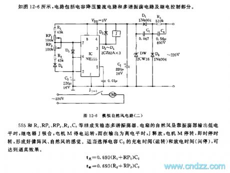
As shown in Figure 12-6, the circuit includes the capacitor step-down rectifier circuit and multivibrator circuit and relay control section. 555 and R1, RP1, RP2, R2, C3 and other components form an astable multivibrator. The natural wind of fan is based on the low oscillator output, the relay J pullling could make the motor M operate, while the output is high, J releases, the motor M stops. That is the motor turns on and off intermittent, and the feeling is like gust, natural wind. Proper selection of charging time and discharging time of capacitor C3 can achieve realistic results.
(View)
View full Circuit Diagram | Comments | Reading(764)
555 simple transistors tester circuit
Published:2011/4/26 1:08:00 Author:Ecco | Keyword: 555 , simple, transistors , tester
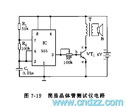
As shown in Figure 7-19, the test instrument is composed of the non-steady-state multivibrator composed of 555 and R1, R2, C1 and the driver of tested grades crystals. It can measure the quality of NPN transistor and estimate B value, the oscillator's oscillation frequency f = 1.44 / (R1 +2 R2) C1. Icon parameter oscillation frequency is about 850Hz. If you plug in the tube, no sound means bad tube; if the sound is small, it indicates that B is low, while loud, B is high.
(View)
View full Circuit Diagram | Comments | Reading(2080)
555 overvoltage, undervoltage delay automatical protection circuit
Published:2011/4/26 1:21:00 Author:Ecco | Keyword: 555 , overvoltage, undervoltage , delay , automatical , protection circuit
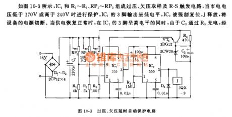
As shown in Figure 10-3, IC1 and R1 ~ R3, RP1 ~ RP3 form overvoltage, undervoltage sampling and R-S trigger circuit, when the mains voltage is below 170V or above 240V, it will be protected in time, IC1's pin 3 output is in low level, IC2 is forced to reset, J releases, power is cut off. When power is restored, pin 3 of IC1 is in high level, C3 is charged through R5, after td = 1.1R5C3, which is about 6 minutes, pin 2is lower than the potential of 1/3 VDD, IC2 sets , J pulls in, the device gets power.
(View)
View full Circuit Diagram | Comments | Reading(1088)
| Pages:41/47 At 2041424344454647 |
Circuit Categories
power supply circuit
Amplifier Circuit
Basic Circuit
LED and Light Circuit
Sensor Circuit
Signal Processing
Electrical Equipment Circuit
Control Circuit
Remote Control Circuit
A/D-D/A Converter Circuit
Audio Circuit
Measuring and Test Circuit
Communication Circuit
Computer-Related Circuit
555 Circuit
Automotive Circuit
Repairing Circuit