
Amplifier Circuits-Audio
Index 10
Internal Block Circuit Diagram of IC LA445
Published:2011/7/7 8:39:00 Author:Vicky | Keyword: Internal Block Circuit Diagram
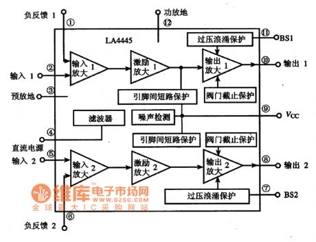
LA445 is a dual-channel audio power amplifier integrated circuit produced by Japanese SANYO Electric. It is widely used in home audio device, vehicle audio device, television audio system, and computer audio System.
Functions and Features
IC LA445 consists of dual-channel audio power amplifier circuit, short-circuit protection circuit, overvoltage protection circuit, surge suppressor circuit, and thermal cutoff circuit. It has various features, such as strong restraining capacity of ripple wave, high separating degree, good balance, and convenient assembling of radiator. It can constitute dual-channel or BTL power amplifier.
The limit working voltage of IC L445 is 25V, maximum quiescent current is 100mA, and typical value is 75mA. Its internal block circuit diagram is shown in the picture. (View)
View full Circuit Diagram | Comments | Reading(1450)
TA8256BH audio power amplifier integrated circuit
Published:2011/7/6 6:06:00 Author:chopper | Keyword: audio power amplifier, integrated circuit
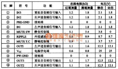
TA8356BH is a new audio power amplifier integrated circuitproduced by Company Toshiba,and it is applied to audio equipment, the multimedia sound,TV acoustics and so on.1.Function characteristics TA8256BH integrated circuits contains three-way audio power amplifier circuit, mute control circuit, and other auxiliary functions circuit. 2 function and data of pins TA8256BH IC adopts 12-pinned single in-line package,and it is used in large-screen TV of Haier Body Strong 34F9BT-TD series, its function and data of pins of the IC are listed in Chart 1.
(View)
View full Circuit Diagram | Comments | Reading(1063)
MC1563 audio power amplifier circuit
Published:2011/7/5 1:14:00 Author:chopper | Keyword: audio, power amplifier
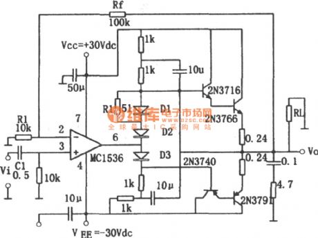
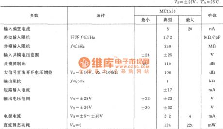
Figure shows the audio power amplifier. The circuit uses a high-voltage, internally-compensated integrated operational amplifier MC1536 .When the supply voltage Vs = ± 36V, the swing amplitude of output voltage is up to ± 30V, the maximum available supply voltage is up to ± 40V, input bias current is small (about 20nA below).The input offset current is less than 3nA, open-loop differential-mode gain is up to 5 × 10⁶ (typical value). The chip is suitable for low-frequency amplification.
(View)
View full Circuit Diagram | Comments | Reading(1007)
simple audio amplifition(LM307、μA741) circuit
Published:2011/7/1 0:08:00 Author:chopper | Keyword: simple, audio amplifition
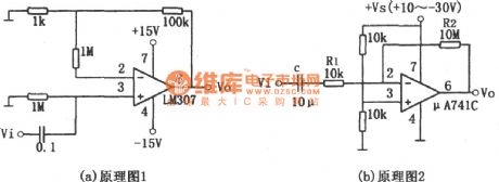
(View)
View full Circuit Diagram | Comments | Reading(1017)
OPA2111 balanced stereo preamplifier circuit
Published:2011/7/1 0:26:00 Author:chopper | Keyword: balanced, stereo, preamplifier
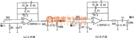
Figure shows a balanced stereo preamplifier circuit. Figure (a) is for the left channel preamplifier circuit,and Figure (b) is for the right channel preamplifier. The circuit uses a dual op-amp OPA2111. Left and right channels, respectively, use a op-amp of dual op-amp OPA2111.Thus the left and right channel have a good matching (gain differ is 3dB, bias differ is 0.5pA, drift differ is ± 0.5μV / ℃), and it is appropriate to constitutes a balanced stereo preamplifier. (View)
View full Circuit Diagram | Comments | Reading(1651)
low-noise preamplifier circuit of OPA37
Published:2011/7/1 0:53:00 Author:chopper | Keyword: low-noise, preamplifier circuit
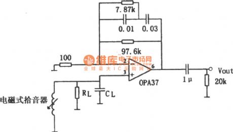
The picture shows the low-noise preamplifier of OPA37. The input signal is applied to OPA37 inverting input (pin 3). RL,CL in the circuit are the load impedances of the electromagnetic pick-up,and their resistances and capacities follow the characteristics of the pick-up(Generally they are based on the recommended parameters ). The all resistors should adopt metal film resistors (1% accuracy), and their capacitors should use organic film capacitors. When the input signal is 1kHz, its gain will be about 100 times. (View)
View full Circuit Diagram | Comments | Reading(1085)
TV remote control 04 circuit
Published:2011/7/2 4:40:00 Author:John | Keyword: TV remote control
View full Circuit Diagram | Comments | Reading(666)
audio firing key amplifition circuit formed by program-controlled op-amp F346
Published:2011/6/30 23:47:00 Author:chopper | Keyword: audio, firing key, amplifition, program-controlled, op-amp
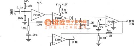
This is a audio firing key amplifition circuit formed by four program-controlled integrated operational amplifier F346.The constant-current source circuit of program-controlled operational amplifier can be controlled by external part,and when constant flow source is loaded to the current bias,the op-amp will be in functional mode,or it will be on cutoff state.Additionally, when the value of current bias is changed,the parameter of the op-amp will be changed,too. (View)
View full Circuit Diagram | Comments | Reading(731)
preamplifier(OPA37) circuit of NAB magnetic head
Published:2011/6/30 2:33:00 Author:chopper | Keyword: preamplifier, NAB magnetic head
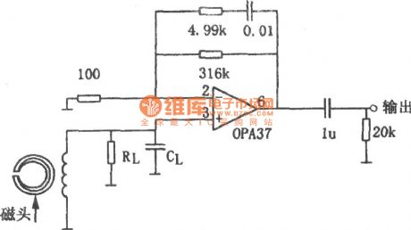
The picture is a preamplifier circuit of NAB magnetic head.This circuit adopts the magnetic head preamplifier formed by ultra-low noise and precise operational amplifier OPA37.This circuit can offer the standard NAB equal.When the frequency is 1kHz,the voltage amplifition time is 50db.The audio input signal is picked by magnetic head device and it is loaded to in-phase input end of OPA37.This connection method can make the operational amplifier possess high input impedance,that is to say,thepath between pin 3 of OPA37 and ground can be taken as a open circuit approximatively.The load impedance of magnetic head is formed by RL,CL and its resistance and capacity can be determined by the features of magnetic head device. (View)
View full Circuit Diagram | Comments | Reading(3149)
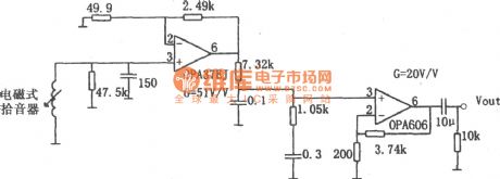
low noise and hifi RIA preamplifier (OPA606) circuit
Published:2011/6/30 2:19:00 Author:chopper | Keyword: low noise, hifi, RIA, preamplifier
(View)
View full Circuit Diagram | Comments | Reading(994)
OPA502 hifi music center amplifition circuit
Published:2011/6/30 2:19:00 Author:chopper | Keyword: hifi, music center, amplifition circuit
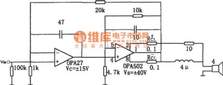
The picture is a hifi music center amplifition circuit.This circuit adopts low noise precise op-amp OPA27 as a preamplifier.The greatest output power can reach 150W.When the output power is 50W and frequency is 20KHz,its total harmonic distortion is 0.02%.And when the frequency is 1KHz,the total harmonic distortion is 0.002%.OPA27 can improve its input impedance by using in-phase input method.When supply voltage is ±15V,the dynamic range of linearity is ±12V.
(View)
View full Circuit Diagram | Comments | Reading(943)
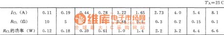
TA7508P karaoke reverberation audio amplifition integrated cirucit
Published:2011/6/17 6:30:00 Author:chopper | Keyword: karaoke, reverberation audio, amplifition, integrated cirucit
TA7508P is a audio amplifition integrated circuit produced by Company TOSHIBA,and it is used as a reverberant acoustics signal generated by amplifition and delay on Konka BT5001 RPTV. TA7508 is one model of the TA7508P integrated circuits whose power is greater than TA7508 and it adopts 35V power supply,while TA7508 adopts 12V power supply.The functions of pins of the two are the same.TA7508 integrated circuit is applied to Konka BT5001 RPTV.Its function and data of integrated circuit is shown as chart 1.
(View)
View full Circuit Diagram | Comments | Reading(739)
audio power amplifier (OPA604) circuit of high-performance but samll power
Published:2011/6/29 0:32:00 Author:chopper | Keyword: audio power amplifier, high-performance, samll power
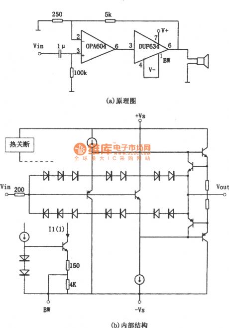
The picture is a audio power amplifition circuit of high-performance but samll power.The preceding stage of circuit adopts FET hi-fi op-amp OPA604,and the backward stage adopts high-speed buffer BUF634, and the voltage will cascade negative feedback between the dual-stage amplifier.The volatge amplifition time is detemined by two resistors(5kΩ and 250Ω) of feedback branch,and their values are 1+5kΩ/250Ω≈21 times.BUF634 is high-speed buffer.The internal structure simplified circuit is shown as picture (b).
(View)
View full Circuit Diagram | Comments | Reading(1216)
LM386 universal audio power amplifier circuit
Published:2011/6/29 0:38:00 Author:chopper | Keyword: universal, audio power amplifier
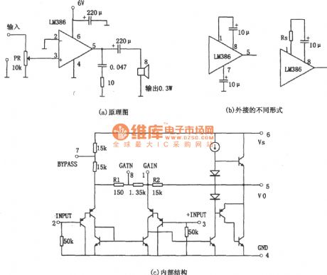
The picture is a universal audio power amplifier circuit.The picture (a) shows the principle,and this circuit adopts integrated power amplifier LM386.This element is a universal power amplifier and it is cheap.The picture (c) shows the inner structure of LM386.
(View)
View full Circuit Diagram | Comments | Reading(1850)
2W audio power amplifier circuit of LM380
Published:2011/6/29 0:55:00 Author:chopper | Keyword: 2W, audio power amplifier
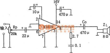
The picture is a 2W audio power amplifier circuit.This circuit adopts 14 pinned LM380 as the amplifier.Add the input signal to the inverting input end(pin 6) of operational amplifier LM380 through the volume control potentiometer Rp(20kΩ) and 22μF coupling capacitor and its in - phase input end (pin 2) is used to earth,pin 1 is circumscribed with 10μF filter capacitor to eliminate the high frequency ripple interference.The circuit adopts 16V single power supply,and circumscribes a 470μF decoupling capacitor between supply end(pin 14) and ground.Between the output end(pin 8) and ground there are two parallel branches.
(View)
View full Circuit Diagram | Comments | Reading(2911)
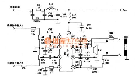
TA7376P dual track power amplification integrated circuit
Published:2011/6/16 1:07:00 Author:chopper | Keyword: dual track, power amplification, integrated circuit
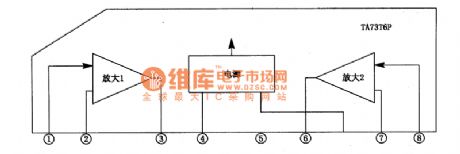
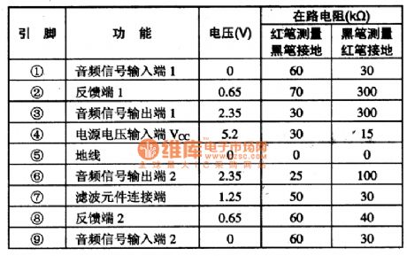
TA7376P is a dual track power amplification integrated circuit and it is of the characteristic that quiescent current is samll,power supply noise is low,output power is big,outward elements are few and so on.The scope of the working power supply is 4.5-9V,typical working voltage is 6V.1.The inner circuit and function of pins of TA7373FThe inner circuit of TA7373F integrated package is shown as picture 1.This IC adopts single inline 9 pinned package.Its function and data of pins are shown as chart 1.
2.TA7376P typical application circuitThe typical application circuit of TA7376P integrated package is shown as picture 2.
(View)
View full Circuit Diagram | Comments | Reading(1141)
TA7232P dual audio power amplifition integrated circuit
Published:2011/6/14 3:32:00 Author:chopper | Keyword: dual audio power, amplifition, integrated circuit
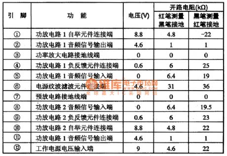
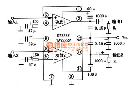
TA7232P is a dual track audio power amplifition integrated circuit produced by Company TOSHIBA,and it is applied to stereo radio and tape player,music center and so on as a power amplifier.1.The inner circuit and function of pins of TA7232PTA7232P integrated package inner circuit is formed by two audio power amplifition circuits of same function.Its integrated package inner circuit and typical application circuit which forms dual track are shown as picture 1.This IC adopts 12 pins single inline package,its function and data of pins of the integrated circuit are shown as chart 1.
(View)
View full Circuit Diagram | Comments | Reading(2827)
TA7215P dual track audio power amplifition integrated circuit
Published:2011/6/16 21:53:00 Author:chopper | Keyword: dual track, audio power, amplifition, integrated circuit
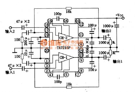
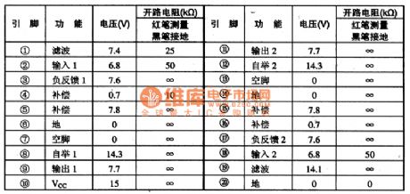
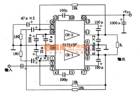
TA7215P is a dual track audio power amplifition integrated circuit,and it is applied to home-use audios and other tape recording players.1.inner circuit and typical application circuitThe inner circuit and typical application circuit of TA7215P integratedcircuit are shown as picture 1.This IC adopts dual inline 20 pinned package.Its function and data of pins of the integrated circuit are shown as chart 1.
2.the main electrical parameter of TA7215PThe scope of working power supply of TA7215P integrated circuit is 4.5-16V.When the load resistance RL=4Ω,THD=10%,f=1KHz,the output power of dual trackis 2.2W if Vcc=9V.
(View)
View full Circuit Diagram | Comments | Reading(2563)
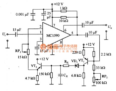
Voice Compression Circuit Diagram formed by MC1590 and Others
Published:2011/6/14 20:48:00 Author:leo | Keyword: Voice Compression Circuit Diagram formed by MC1590 and Others, MC1590
View full Circuit Diagram | Comments | Reading(3525)
The high voltage input FET power amplifier circuit diagram
Published:2011/6/10 22:01:00 Author:leo | Keyword: The high voltage input FET power amplifier circuit diagram, 2SA639, 2SC1279, 2SA818, 2SA633, 2SC1628
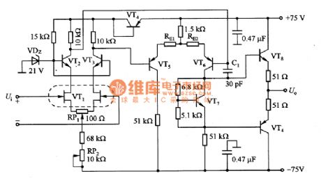
As the picture 1 shows, it is a high voltage input power amplifier circuit. The input VT1 of the circuit adopts FET tube. And its drain is connected to common base amplifier formed by VT2 and VT3, which is used to electric level move in order to prevent high voltage from being connecting to the drain of VT1. VT5 and VT6 are differential amplifying circuit.When the emitter is connect is added the current feedback, convert rate will be improved. Feedback resistance value of RE1 and RE2 need to be 0 to 5OOΩ. VT4 should be connected to be a diode which is used to make up the difference of UBE of VT5 and VT^ causing by temperature changes. VT8 and VT9 are push-pull output circuit. (View)
View full Circuit Diagram | Comments | Reading(4671)
| Pages:10/13 12345678910111213 |
Circuit Categories
power supply circuit
Amplifier Circuit
Basic Circuit
LED and Light Circuit
Sensor Circuit
Signal Processing
Electrical Equipment Circuit
Control Circuit
Remote Control Circuit
A/D-D/A Converter Circuit
Audio Circuit
Measuring and Test Circuit
Communication Circuit
Computer-Related Circuit
555 Circuit
Automotive Circuit
Repairing Circuit