
Index 160
LOGARITHMIC_AMPLIFIER_1
Published:2009/6/23 2:51:00 Author:Jessie
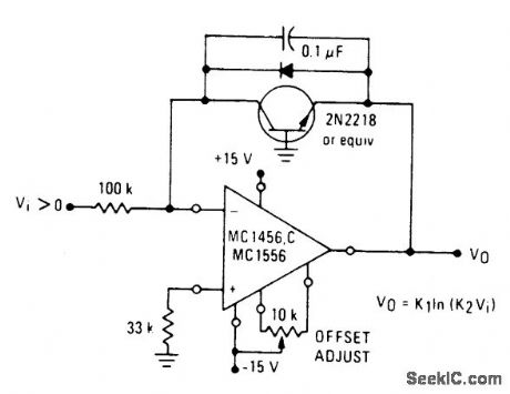
View full Circuit Diagram | Comments | Reading(646)
WIDEBAND_UNITY_GAIN_INVERTING_AMPLIFIER_IN_A_75_OHM_SYSTEM
Published:2009/6/23 2:49:00 Author:Jessie
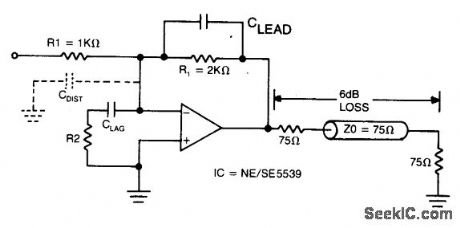
View full Circuit Diagram | Comments | Reading(685)
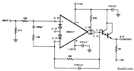
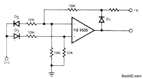
INVERTING_AMPLIFIER__WITH_BALANCING_CIRCUIT_
Published:2009/6/23 2:13:00 Author:May
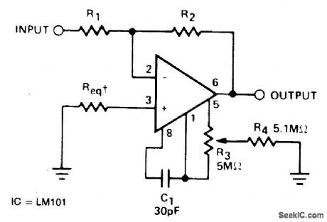
Req may be zero or equal to parallel combination of R1 and R2 for minimum offset. (View)
View full Circuit Diagram | Comments | Reading(687)
×1000_AMPLIFIER_CIRCUIT
Published:2009/6/23 2:11:00 Author:May
View full Circuit Diagram | Comments | Reading(610)
AMPLIFIER_COOL_DOWN_CIRCUIT_I
Published:2009/6/23 2:25:00 Author:Jessie
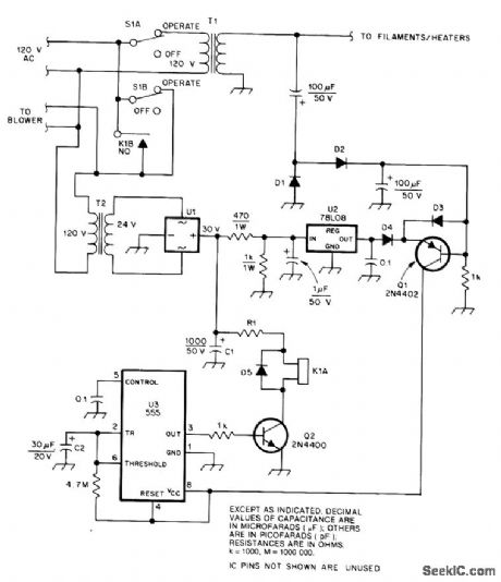
This cool-down relay circuit uses an IC timer to drive a relay, which keeps the blower on for a time delay from timer U3. The value of C2 can be changed to lengthen or shorten the time, as needed. (View)
View full Circuit Diagram | Comments | Reading(1463)
COMPLEMENTARY_OR_BILATERAL_ac_EMITTER_FOLLOWER_CIRCUIT
Published:2009/6/23 2:20:00 Author:Jessie
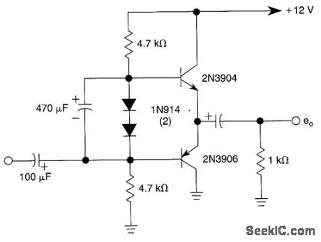
This noninverting circuit uses a pair of com-plementary npn (2N3904) and pnp (2N3906) transistors. (View)
View full Circuit Diagram | Comments | Reading(3111)
LOGARITHMIC_AMPLIFIER
Published:2009/6/23 1:59:00 Author:May
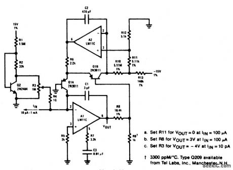
Unusual frequency compensation gives this logarithmic converter a 100 μs time constant from 1 mA down to 100 μA, increasing from 200 μs to 200 ms from 10 nA to 10 pA. Optional bias current compensation can give 10 pA resolution from - 55 ℃ to 100 ℃, Scale factor is 1 V/decade and temperature compensated. (View)
View full Circuit Diagram | Comments | Reading(821)
VOLTAGE_CONTROLLED_VARIABLE_GAIN_AMPLIFIER
Published:2009/6/23 1:56:00 Author:May
The tee attenuator provides for optimum dynamic linear range attenuation up to 100 dB, even at f = 10.7 MHz with proper layout. (View)
View full Circuit Diagram | Comments | Reading(3021)
UNITY_GAIN_FOLLOWER
Published:2009/6/23 1:55:00 Author:May
View full Circuit Diagram | Comments | Reading(698)
HIGH_IMPEDANCE_DIFFERENTIAL_AMPLIFIER
Published:2009/6/23 1:54:00 Author:May
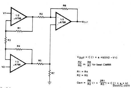
View full Circuit Diagram | Comments | Reading(1713)
500_ksps_8_CHANNEL_DATA_DCQUISITION_CIRCUT
Published:2009/6/23 2:10:00 Author:Jessie
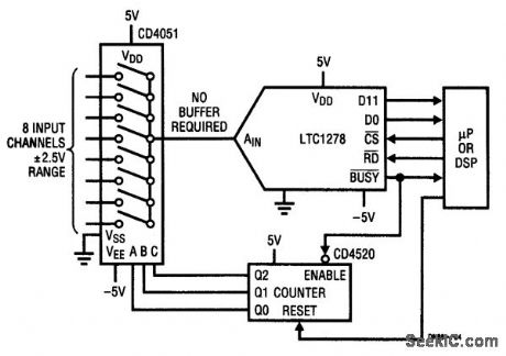
The high input impedance of the LTC1278 allows multiplexing without abuffer amplifier. Both sin-gle channel and multiplexed high-speed data acquisition systems benefit from the LTC1278/LTC1279's dynamic conversion performance. The 1.6-μs and 1.4-μs conversion and 200-ns and 180-ns S/H acquisition times enable the LTC1278/LTC1279 to convert a 500 ksps and 600 ksps, respectively. The figure shows a 500-ksps 8-channel data acquisition system. The LTC1278's high input impedance eliminates the need for a buffer amplifier between the multiplexer's output and the Adc's input. (View)
View full Circuit Diagram | Comments | Reading(1398)
PROGRAMMABLE_GAIN_NONINVERTINGAMPLIFIER_WITH_SELECTABLE_INPUTS
Published:2009/6/23 2:08:00 Author:Jessie
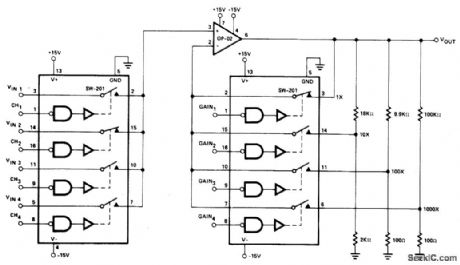
View full Circuit Diagram | Comments | Reading(1214)
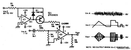
ABSOLUTE_VALUE_AMPLIFIER
Published:2009/6/23 2:07:00 Author:Jessie
The circuit generates a positive output voltage for either polarity of input. For positive signals, it acts as a noninverting amplifier and effective. The accuracy is poor for input voltages under 1 V, but for less stringernt applications, it can ve effective. (View)
View full Circuit Diagram | Comments | Reading(1896)
VOLTAGE_CONTROLLED_AMPLIFIER
Published:2009/6/23 2:04:00 Author:Jessie
This circuit is basically an op amp with an extra input at pin 5. A current Ltac is injected into this input and this controls the gain of the device linerly. Thus by inserting an audio signal (±10 mV) between pin 2 and 3 and by controlling the current on pin 5, the level of the signal output (pin 6) is controlled. (View)
View full Circuit Diagram | Comments | Reading(3502)
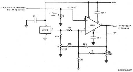
PRECISION_PROCESS_CONTROL_INTERFACE
Published:2009/6/23 2:03:00 Author:Jessie
View full Circuit Diagram | Comments | Reading(1123)
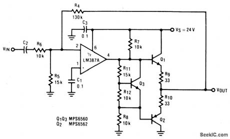
DISCRETE_CURRENT_BOOSTER
Published:2009/6/23 2:02:00 Author:Jessie
View full Circuit Diagram | Comments | Reading(1374)
VOLTAGE_CONTROLLED_VARIABLE_GAIN_AMPLIFIER_1
Published:2009/6/23 2:01:00 Author:Jessie
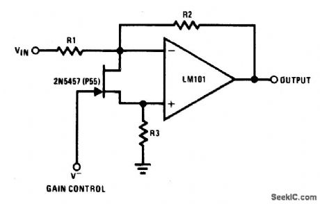
The 2N5457 acts as a voltage variable resistor with an Rds(on) of 800 ohms max. Since the differential voltage on the LM101 is in the low mV range, the 2N5457 JFET will have linear resistance over several decades of resistance providing an excellent electronic gain control. (View)
View full Circuit Diagram | Comments | Reading(2891)
PREAMP_TRANSMIT_RECEIVE_SEQUENCER
Published:2009/6/23 1:41:00 Author:Jessie
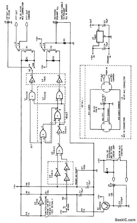
This circuit is useful in amateur radio VHF and UHF work where a mast-mounted antenna preamp is used for receiving. The kit controls T-R switching and change-over relay sequencing so that high RE levels are prevented from accidentally being applied to the preamplifier during switching intervals. (View)
View full Circuit Diagram | Comments | Reading(1665)
Adjustable Rate Constant Sinusoidal Frequency Oscillator Circuit
Published:2011/7/18 5:40:00 Author:Felicity | Keyword: Adjustable Rate Constant, Sinusoidal Frequency Oscillator, Circuit
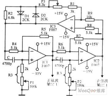
Adjustable Rate Constant Sinusoidal Frequency Oscillator Circuit is showed in the picture above. (View)
View full Circuit Diagram | Comments | Reading(646)
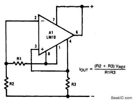
CURRENT_REGULATOR_OP_AMP
Published:2009/6/22 23:35:00 Author:May
View full Circuit Diagram | Comments | Reading(756)
| Pages:160/250 At 20141142143144145146147148149150151152153154155156157158159160Under 20 |
Circuit Categories
power supply circuit
Amplifier Circuit
Basic Circuit
LED and Light Circuit
Sensor Circuit
Signal Processing
Electrical Equipment Circuit
Control Circuit
Remote Control Circuit
A/D-D/A Converter Circuit
Audio Circuit
Measuring and Test Circuit
Communication Circuit
Computer-Related Circuit
555 Circuit
Automotive Circuit
Repairing Circuit