
Index 161
SINGLE_SUPPLY_OP_AMP_APPLICATIONS
Published:2009/6/22 23:34:00 Author:May
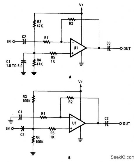

An op amp that normally needs two supplies can be used when only a single supply is needed. The value of V+ should be twice the minimum allowable values of the positive and negative voltages normally needed. For example, a 12-V single-supply application would require an op amp capable of ±6-V operation. (View)
View full Circuit Diagram | Comments | Reading(2114)
PARALLELED_POWER_OP_AMPS
Published:2009/6/22 23:30:00 Author:May
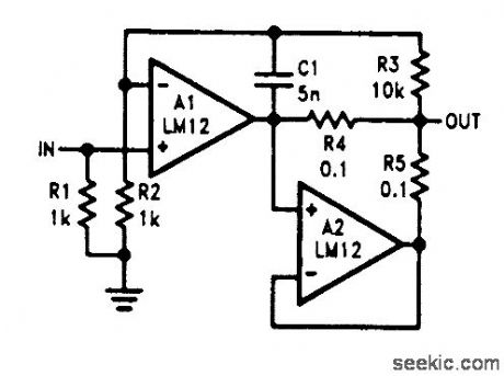
Two power op amps can be paralleled using this master/slave arrangement, but high-requency performance suffers. (View)
View full Circuit Diagram | Comments | Reading(661)
ENHANCED_OP_AMP_BALANCED_AMPLIFIER
Published:2009/6/22 23:29:00 Author:May
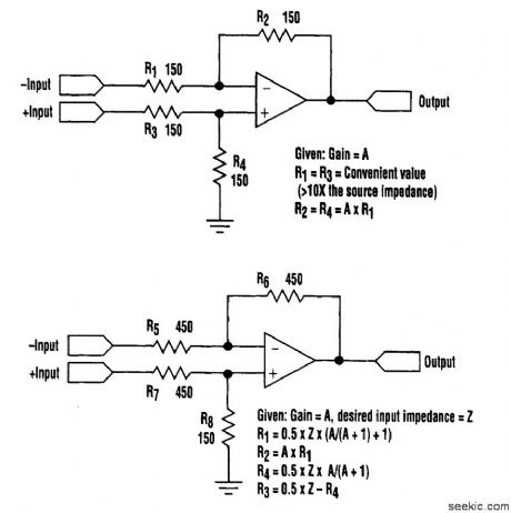
The classic single op-amp balanced circuit works well in low-source-impedartce configurations, but tends to struggle in higher-source-imp edance applications because of the varying input impedance of the inputs referred to ground.
A modified version of the classic op-amp configuration of the figure uses a different set of formulas to determine the resistor values. It equalizes the impedance of both inputs by considering the op amp's active participation. (View)
View full Circuit Diagram | Comments | Reading(2882)
INPUT_GUARDING_FOR_HI_ZOP_AMPS
Published:2009/6/22 23:27:00 Author:May
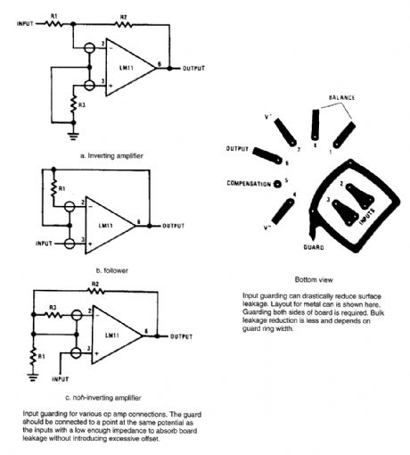
View full Circuit Diagram | Comments | Reading(691)
BASIC_OP_AMP_AUDIO_AMPLIFIER
Published:2009/6/22 23:26:00 Author:May
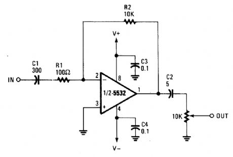
Any general-purpose op amp can be used in this application. (View)
View full Circuit Diagram | Comments | Reading(4063)
PSEUDOGROUND
Published:2009/6/22 23:37:00 Author:Jessie
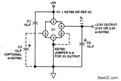
For op-amp circuits, a pseudo ground is often needed; a voltage reference IC can be used. The Analog Devices AD780 is used here for this application. This can sink or source current. (View)
View full Circuit Diagram | Comments | Reading(1663)
OP_AMP_RESISTANCE_MULTIPLICATION_CIRCUIT
Published:2009/6/22 23:36:00 Author:Jessie
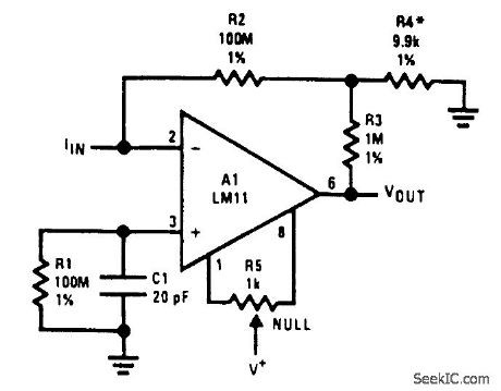
Equivalent feedback resistance is 10 GΩ, but only standard resistors are used. Even though the offset voltage is multiplied by 100, output offset is actually reduced because error is dependent on offset current, rather than bias current. Voltage on summing junction is less than 5 mV. (View)
View full Circuit Diagram | Comments | Reading(900)
The current sensor applied connector circuit
Published:2011/7/21 2:34:00 Author:Seven | Keyword: current sensor, applied connector
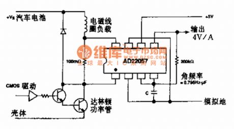
Function: it is used in the current sensor, motor control, accelerating sensor, pressure sensor, position symbol sensor, strain sensor and other low LEV signal source circuits.
(View)
View full Circuit Diagram | Comments | Reading(613)
OP_AMP_OFFSET_NULL
Published:2009/6/22 23:24:00 Author:Jessie
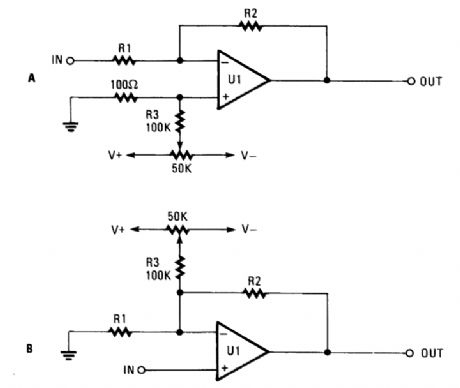
Offset problems can occur in the best of circuits (and often do) without regard to whether the circuit is inverting (A), or noninverting (B). Offset-nulling potentiometers are useful in correcting the output to zero, but their effectiveness will vary under different conditions. (View)
View full Circuit Diagram | Comments | Reading(1113)
OP_AMPS_WITH_LONG_RC_TIME_CONSTANTS
Published:2009/6/22 23:22:00 Author:Jessie
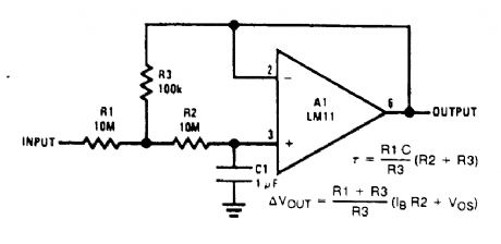

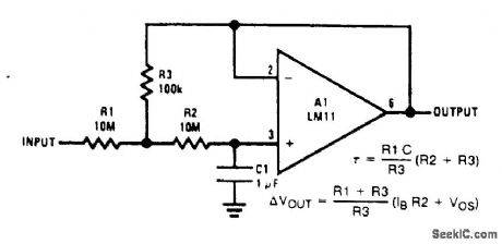
This circuit multiplies RC time constant to 1000 seconds and provides low output impedance.Cost is lowered because of reduced resistor and capacitor values. (View)
View full Circuit Diagram | Comments | Reading(780)
BASIC_OP_AMP_CIRCUITS
Published:2009/6/22 23:21:00 Author:Jessie
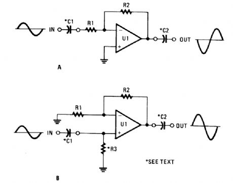
The two simplest op-amp configurations are the inverting (A) and the noninverting (B). Resistor R3 is needed only if C1 is used in the noninverting circuit. (View)
View full Circuit Diagram | Comments | Reading(1018)
The reset stable amplifier(wave chopper amplifier) circuit
Published:2011/7/24 7:59:00 Author:Seven | Keyword: stable amplifier, wave chopper amplifier
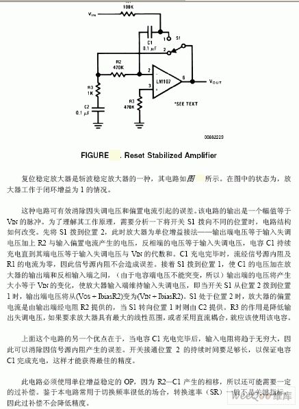
The reset stable amplifier is one kind of wave chopper amplifier, whose circuit is shown in the figure, the amplifier works in the environment where the close loop gain is 1.The circuit can effectively remove the fault caused by offset voltage and bias current. The output of the circuit is a pulse whose amplitude is Vin. To understand its working principle, there is the need to analyse the circuit structure change when the switch S1 is pulled to different position. (View)
View full Circuit Diagram | Comments | Reading(686)
The 555 linear PWM circuit
Published:2011/7/20 7:47:00 Author:Seven | Keyword: linear PWM circuit
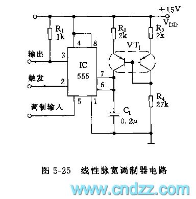
See as figure 5-25, IC(555), R2, VT1 and C1 compose the controllable single steady circuit, the contemporary pulse wavelength is in backward proportion to the input modulation signal, the higher the modulation LEV is, the narrower the pulse will be. VT1 is a symmetric dual triode BT51, which composes the mirror image current source with R2 and R3, and the mirror image makes the charge current of C1 keep linear in the contemporary stable period, the linearity is ±0.2%.
(View)
View full Circuit Diagram | Comments | Reading(1125)
TELEPHONE_AMPLIFIER
Published:2009/6/22 22:57:00 Author:May
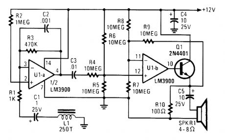
Section UI-a is configured as a high-gain inverting voltage amplifier that is inductively coupled to the phone line via L1. Inductor L1 is a homemade unit that consists of 250 turns of fine, enamel-coated wire that is wound on an iron core. The op amp receives the few mV produced by L1 via C1 and RI and amplifies the signal. Capacitor C1 acts as the negative-feedback component that limits the circuit's high-frequency gain, while R3 limits the low-frequency gain. Resistor R3 is particularly important because without it, the amplifier would saturate.Op amp UI-b is configured as a difference amplifier. It receives a signal from U1-a via C3 and R4 and amplifies the difference between it and half of the supply voltage. Transistor Q1 is configured as a common-collector amplifier ensuring sufficient signal to drive the speaker. Capacitor C5 is used to remove any dc component provided by transistor Q1. (View)
View full Circuit Diagram | Comments | Reading(1878)
MOSFET high frequency amplifier circuit diagram
Published:2011/3/30 22:20:00 Author:Ecco | Keyword: high frequency amplifier
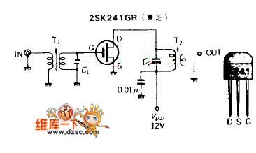
The preamplifier(1) VHF high frequency amplifier circuit of unipole gate polar MOS FET is based on Bipolar Transistor, but mostly replaced by the FET now. Figure 2-1 is its typical circuitry, 2SK241(Toshiba) adopts FET to increase its gaining power to 28dB(@100MHz). And it is suitable for VHF receiver to amplifier its frequency class. As been zero bias on operating point, the structure of the circuitry is simple, the whole components is 6. Figure 2-1shows a inductance and capacitance which can apply in different kinds of high frequency amplifiers. When the polar current is 9mA, the current will keep constant with the voltage in the range of 6~12V.
(View)
View full Circuit Diagram | Comments | Reading(3266)
The 555 linear voltage/frequency converter circuit
Published:2011/7/20 7:37:00 Author:Seven | Keyword: voltage/frequency converter
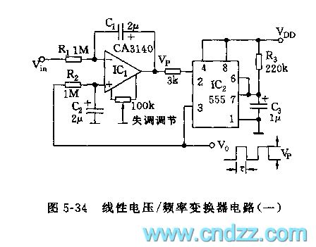
See as figure 5-34, the linear voltage/frequency converter consists of a differentiation/integration circuit and a single stable trigger delay circuit, which is used in voltage/frequency conversion. The IC is a MOSFET computing amplifier CA3140(OR 4573), which forms the integration circuit of the differentiation input, its output terminal control is added to the trigger of IC2, the output of the single stable trigger circuit is added to the non-inverting terminal of the integrator, by changing the integral phase, the output of IC1, a triangular wave, increases or decreases in linearity.
(View)
View full Circuit Diagram | Comments | Reading(3036)
The 555 quadruple frequency multiply circuit
Published:2011/7/20 7:28:00 Author:Seven | Keyword: quadruple frequency, multiply circuit
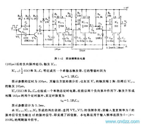
This multiply circuit can convert the period sequence of f1 into output pulse signal of f0=4f1, which is a quadruple frequency circuit, see as figure 5-42. The circuit includes the differentiation twice frequency circuit, single stable timing circuit and double frequency circuit and so on. VT1, R1, C1, C2 and R2 compose the phase inverting amplifier and differentiation circuit. C2, R2 and C1, R2 compose the differentiation circuit which forms 2 undershoot narrowing pulses, the first doubling is done at the collecting electrode of VT2.
(View)
View full Circuit Diagram | Comments | Reading(776)
555 as the D power amplifier circuit
Published:2011/7/20 7:16:00 Author:Seven | Keyword: power amplifier
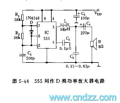
See as figure 5-44, IC(555), R1, R2 and C1 compose a controllable multi-resonance oscillator whose frequency is 100KHz, duty cycle is 50%. The control terminal 5-pin is added with an audio signal, then the output of 3-pin is a PWM pulse signal whose PWM is in forward proportion to the amplitude. After filtering by L and C3, an amplified audio signal is got.
(View)
View full Circuit Diagram | Comments | Reading(2520)
The 555 dual electric door bell circuit (1)
Published:2011/7/20 7:58:00 Author:Seven | Keyword: electric door bell
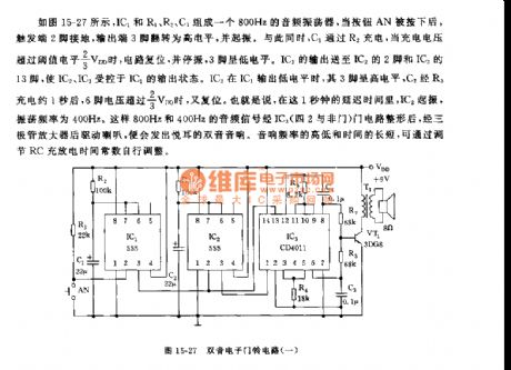
See as figure 15-27, IC1, R1, R2 and C1 compose a 800Hz audio oscillator circuit, when AN is pressed, the 2-pin of the trigger is connected with the earth, the 3-pin of the output terminal is reversed to be in a high LEV and starting to oscillate. Meanwhile, C1 is charged by R2, when the charge voltage is over the threshold LEV of 2/3VDD, the circuit is reset and stopping oscillating, the 3-pin is in a low LEV. The output of IC1 is sent to the 2-pin of IC2 and 13-pin of IC3, which makes IC2 and IC3 to be controlled by the output state of IC1.
(View)
View full Circuit Diagram | Comments | Reading(968)
BUFFER_FOR_A_D_CONVERTERS
Published:2009/6/22 22:47:00 Author:Jessie
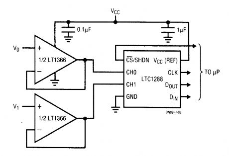
This circuit uses an LT1366 driving an LTC1288 two-channel micropower A/D. The LTC1288 can accommodate voltage references and input signals equal to the supply rails. The sampling nature of this A/D eliminates the need for an external sample-and-hold, but might call for a drive amplifier be-cause of the A/D's 12-ps settling requirement. The LT1366's rail-to-rail operation and low-input off-set voltage make it well suited for low-power, low-frequency A/D applications. In addition, the op-amp's output settles to 1% in response to a 3-mA load step through 100 pF in less than 1.5μs. (View)
View full Circuit Diagram | Comments | Reading(1646)
| Pages:161/250 At 20161162163164165166167168169170171172173174175176177178179180Under 20 |
Circuit Categories
power supply circuit
Amplifier Circuit
Basic Circuit
LED and Light Circuit
Sensor Circuit
Signal Processing
Electrical Equipment Circuit
Control Circuit
Remote Control Circuit
A/D-D/A Converter Circuit
Audio Circuit
Measuring and Test Circuit
Communication Circuit
Computer-Related Circuit
555 Circuit
Automotive Circuit
Repairing Circuit