
Index 177
LM1876 Power Amplifier Circuit
Published:2011/7/15 20:23:00 Author:Robert | Keyword: Power, Amplifier
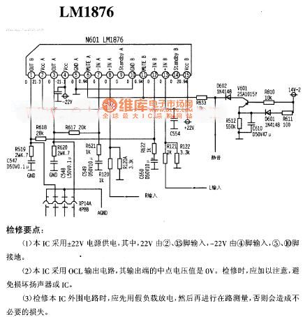
The picture shows the LM1876 power amplifier circuit.
Maintenance points:
(1)This IC uses +/-22V power supply. The 22V should input to pin 2 and pin 15 and the -22V should input to pin 4. The pic 5 and pin 10 should be connected to the ground.
(2)This IC uses OCL output circuit and the output port's middle point's voltage is 0V. When this circuit needs maintenance it should be noticed to avoid to damage the speaker or IC.
(3)When the IC's external circuit needs maintenance it should use a dummy load for discharging and then do the measurement on the circuit. Otherwise it may cause unnecessary damage. (View)
View full Circuit Diagram | Comments | Reading(6302)
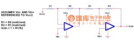
In-Phase Summation Circuit
Published:2011/7/16 6:46:00 Author:Robert | Keyword: In-Phase, Summation
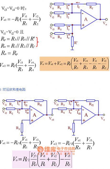
1.This is the in-phase summation circuit.
With the concepts of virtual short circuit and virtual open circuit, we get the single operational amplifier summation-difference circuit anddual operational amplifier summation-difference circuit. (View)
View full Circuit Diagram | Comments | Reading(921)
Addition And Subtraction Operation Circuit
Published:2011/7/16 6:53:00 Author:Robert | Keyword: Addition, Subtraction, Operation
1.Out-phase summation circuit.
Virtual short circuit and virtual open circuit.
Feature:if adjusting one channel signal's input resistance it would not affect other channel's input and output ratio.
2.In-phase summation circuit.
Virtual short circuit and Virtual open circuit. (View)
View full Circuit Diagram | Comments | Reading(591)
LM4915 Used In Double-Channel Amplification Circuit
Published:2011/7/16 8:09:00 Author:Robert | Keyword: Double-Channel, Amplification
The picture shows the LM4915 used in double-channel amplification circuit. The left, right sound-channel signals would input to the LM4915's pin 8 and pin 3 separately. After the internal amplifier's amplification the signals would output from the pin 6 and pin 5 separately and then coupling on their own sound-channel speaker directly. The LM4915 amplifier gain is determined by its internal resistance Ri and Rf and the internal certain gain is set to 6dB. The amplifier's maximum power consumption would be PDMAX=4VDD2/π2RL in push-pull output coupling mode and would be PDMAX=VDD2/π2RL in single-port output coupling mode. fc=1/2πRiCi and the Ri=20kΩ. The LM4915's pin 1 is connected external closing control switch. When the pin 1 is connected to high voltage level, (1.8V could be high voltage level), it would allow to work. When the pin 1 is connected to low voltage level, (0.4V could be low voltage level), it would prohibit working to reduce the chip's power consumption. (View)
View full Circuit Diagram | Comments | Reading(597)
Differential Input Amplifier Circuit With Common-Mode Voltage Up To ±100V
Published:2011/7/16 8:59:00 Author:Robert | Keyword: Differential, Input, Amplifier, Common-Mode Voltage, ±100V
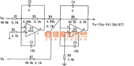
The picture shows the differential input amplifier circuit with common-mode voltage up to ±100V. In practical applications, sometime it needs the amplifier to have high common-mode voltage (±100V). For enhancement of this feature, it offen needs to sacrific some other features. The differential input amplifier circuit, which could achieve that the common-mode voltage is up to ±l00V, is shown in the picture. This circuit's voltage gain is only equal to 1. The circuit uses two common integrated single operational amplifiers 301.
The table shows the 301 integrated operational amplifier's main parameters (typical value). (View)
View full Circuit Diagram | Comments | Reading(763)
Differential Output Amplification Circuit
Published:2011/7/17 8:21:00 Author:Robert | Keyword: Differential, Output, Amplification
The picture shows the differential output amplification circuit. (View)
View full Circuit Diagram | Comments | Reading(603)
Class AB Amplification Complementary Symmetry Circuit
Published:2011/7/15 20:08:00 Author:Robert | Keyword: Class AB, Amplification, Complementary, Symmetry
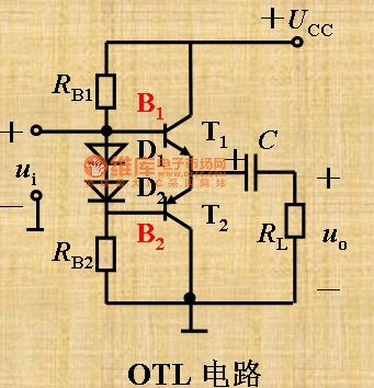
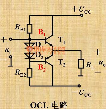
The picture shows the class AB amplification complementary symmetry circuit.
The circuit picture shows the OTL circuit. The second picture shows the OCL circuit.
These circuits have the following features:
(a)By adding RB1, RB2 it provides a certain bias current to avoid the crossover distortion.
(b)By adding diode D1, D2 it could make the B1 point and B2 point keep different voltage level in static mode and it could send the ui signal to the B1, B2 points successfully in dynamic mode. (View)
View full Circuit Diagram | Comments | Reading(922)
Video amplifier circuit
Published:2011/7/14 22:02:00 Author:zj | Keyword: Video amplifier
View full Circuit Diagram | Comments | Reading(611)
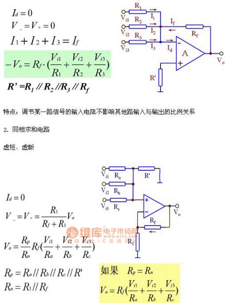
Single Operational Amplifier Basic Subtraction Circuit Composed Of LM158
Published:2011/7/16 21:02:00 Author:Robert | Keyword: Single, Operational Amplifier, Basic, Subtraction
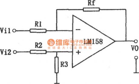
The picture shows the single operational amplifier basic subtraction circuit.
To avoid the error caused by the bias current, it is required that the external circuit total resistance value of the operational amplifier's two input ports should be balanced.
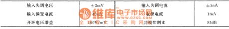
This circuit uses the element of LM158. It is a single-chip high-gain dual operational amplifiers which would work under a wide range of single power supply. Its power current would be small and would have no relations to the power voltage. The LM158's main parameters are listed in the table. (View)
View full Circuit Diagram | Comments | Reading(919)
The low-light amplifier circuit diagram
Published:2011/5/13 4:13:00 Author:Ecco | Keyword: low-light amplifier
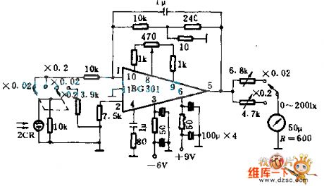
This circuitry is usedas the amplifier circuitry that the range is 21X and 20 IX, if the range is higher than 200 IX, it can be settled by paralleling connecting resistance by a header directly. In order to assure linear feature, when it measures a 20 IX tick, the burdenof 2 CR diminishes because of paralleling connecting resistor in 3.9 K Ω, and the error is about ±4%; The stability changes ±endless% annually, but it is effected by temperature, and increasing 1 ℃ JF each time, the value will enlarge 1%.
(View)
View full Circuit Diagram | Comments | Reading(704)
The wiring circuit diagram with single-phase watt-hour meter measuring electric power
Published:2011/5/13 3:10:00 Author:Ecco | Keyword: wiring circuit , single-phase , watt-hour meter , measuring , electric power
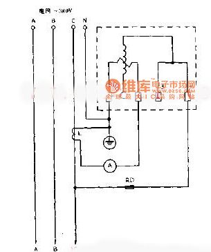
Three-phase AC power used in rural areas and plant is mainly used as electrical power for motor, it generally requires a three-phase meter. If there is only single-phase power meter, the wiring method is as the diagram, it can measure three-phase meter electricity consumption by the single-phase meter, the former single-phase watt-hour meter reading is multiplied by 3, that is the actual consumption of three-phase power.
(View)
View full Circuit Diagram | Comments | Reading(2355)
Loop elimination, cold junction compensation and high-end thermocouple amplifier circuit diagram
Published:2011/6/23 2:41:00 Author:Ecco | Keyword: Loop elimination, cold junction compensation , high-end , thermocouple amplifier
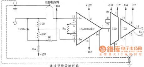
The loop elimination, cold junction compensation and high-end thermocouple amplifier circuit composed of ISO102 and INA101are shown as the chart, it has the fuctions of ground loop elimination, cold junction compensation and high-end off. This circuit uses the K thermocouple to test temperature in the field, the temperature signal is converted to voltage signal, amplified by instrumentation amplifier INA101 and sent to ISO102, isolated and amplified, output by ISO102. Resistor Rc is used to set the INA101's gain. The feature of circuit is that K thermocouple is connected to the ground of ISO102 secondary side, then it will form the same potential, thereby it eliminates the interference caused by ground loop.
(View)
View full Circuit Diagram | Comments | Reading(1926)
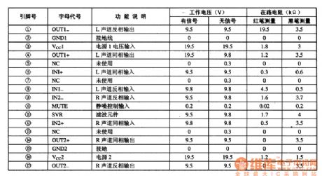
TDA8946J pin functions and power amplification circuit diagram
Published:2011/6/27 2:17:00 Author:Ecco | Keyword: pin functions , power amplification
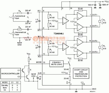
TDA8946J is a dual audio power amplifier, which contains two BTL amplifier circuits. When the power supply voltage is 18V, the load is 8 ohms, it can output 2 X 15W effective power. TDA8946J is packaged with ZIP dual in-line with the power supply range in 6 ~ 25V. THD total harmonic distortion is 0.03 0.1. 1. negative output terminal; 2. ground; 3. supply voltage VCC1; 4. output terminal; 5. empty; 6. the input signal; 7. empty; 8. input 1 is negative; 9. signal input 2 is negative; 10 . squelch control (alternate); 11. ripple rejection (external connected 10nF capacitor to ground); 12. signal input 2 is positive ; 13. empty; 14. output terminal 2 is negative; 15. ground; 16. power supply voltage VCC2; 17. output Terminal 2 is positive.
(View)
View full Circuit Diagram | Comments | Reading(5591)
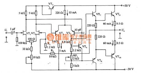
Class A discrete component amplifier circuit diagram
Published:2011/6/26 21:58:00 Author:Ecco | Keyword: Class A , discrete component , amplifier
This amplifier circuit uses the dual 20V power supply voltage to provide 15W power without distortion at the 8 ohm load. Q1 operates in the common emitter, and the input signal can provide constant current bias through the bias tube, which is including Q8, Q9, D6, D13 and D14. Q8 and Q9, and the product phase is minimized by the separation darlington tubes (Q2, q4) and (Q7, q11). The two transistors uses Transitors, specifically the types of 2N3055 and MJ2955. R16 uses the series of 4.7K, 680 Ohms and 820 ohm resistors.
(View)
View full Circuit Diagram | Comments | Reading(1001)
TDA8944J two-channel BTL audio power amplifier integrated circuit diagram
Published:2011/6/23 2:49:00 Author:Ecco | Keyword: two-channel , BTL, audio, power amplifier, integrated circuit
TDA8944J is two-channel BTL audio power amplifier integrated circuit produced by Philips company, it is widely used in various high-fidelity home theater, television, stereo, computer audio. 1. Function descriptionTDA8944J IC has two BTL audio power amplifier circuits with the the same function, it also has a switch function of static noise, and thermal protection, short circuit protection circuit. When the working voltage is 12V, RL = 8Ω, each channel output power is 7W. 2. IC pin functions and data TDA8944J uses 17-foot single-line package, the pin functions and data are listed in Table 1. Table 1 shows TDA8944J pin function integrated circuit and data.
(View)
View full Circuit Diagram | Comments | Reading(4607)
Negative feedback ultra-linear amplifier circuit diagram
Published:2011/6/27 2:21:00 Author:Ecco | Keyword: Negative feedback, ultra-linear , amplifier
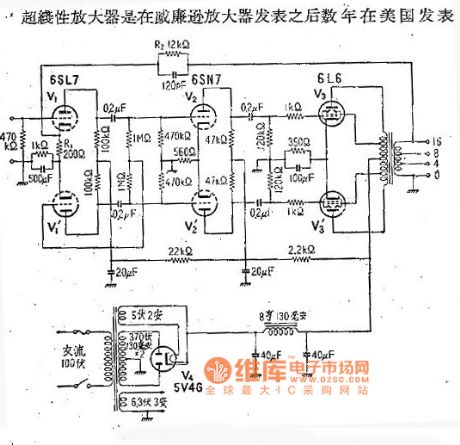
The ultra-linear amplifier is published after several years of Williamsonamplifier.
(View)
View full Circuit Diagram | Comments | Reading(1092)
ULN2204,LN2204A,LN2204A 21 single chip audio integrated circuit
Published:2011/7/13 20:00:00 Author:leo | Keyword: Single chip, Audio, Integrated circuit
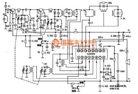
ULN204, ULN2204A and ULN2204A—21 are a kind of single chip audio integrated circuit used in pocket-sized radio and other kinds of radios.
1.ULN2204 integrated chip inner circuit diagram and pin functions:ULN2204 AM part contains AGC, MIX, LO, ZF and detecting circuit. The AM part does not include AGC and MIX circuit but only ZF and frequency discrimination circuit. Its pin functions are shown in the picture.
2.ULN2204 main parameters:The integrated circuit ULN2204 has a operating power supply voltage coverage of 3 V to 12 V with the classic voltage of 4.5 V.(1)When Ta is 25℃ and Vcc is 13V, the power consumption P(D) is 600 mW and current I(REY) is 60 mA.(2)Other main parameters are shown in the picture. (View)
View full Circuit Diagram | Comments | Reading(3868)
Op amp instrumentation circuit diagram
Published:2011/6/24 2:36:00 Author:Ecco | Keyword: Op amp , instrumentation
In many cases, the op amp input end is connected to the capacitor to prevent DC level caused by virtual ground. This capacitor is actually a high-pass filter, in a sense, all single-supply op amp circuits like this have such a capacitor. Filter implementation is simple, but the designer must pay attention to the following points: 1. Filter inflection point (center) frequency; 2. the gain of the filter circuit; 3. Q value of of bandpass filter and band stop filter; 4. low-pass and high-pass filter types (Butterworth, Chebyshev, Bessell).
(View)
View full Circuit Diagram | Comments | Reading(555)
FET DC power amplifying circuit
Published:2011/7/13 20:04:00 Author:leo | Keyword: FET, DC power amplifying, Circuit
Picture 1 shows a FET DC power amplifying circuit. VT1 is the difference amplifying circuit, while VT2 is the constant current differential circuit. And VT5 is electrical level moving circuit made by cascading amplifiers. The source voltage of VT3 is about 0.6 V and VT7 and VT8 are current mirror circuit which is used to aggrandize gain and improve the DC operating point stability. VT6 is the circuit that offers differential current to output terminal.
(View)
View full Circuit Diagram | Comments | Reading(970)
A FET audio amplifying circuit
Published:2011/7/13 20:05:00 Author:leo | Keyword: FET, Audio, Amplifying circuit
Picture 1 shows a FET audio amplifying circuit which demands small distortion, broad frequency bandwidth. The input terminal uses Knot type FET which can eliminate the influence to circuit caused by change of source voltage and current moving. DC stability is the main problem of direct-coupling DC amplifier which needs to use two level difference circuits. The first level difference circuit is formed by N channel FET, VT1 and VT2. The second level difference circuit is formed by PNP, VT4 and VT5, which has a high voltage amplitude of vibration and bigger distortion that should be paid attention during design. (View)
View full Circuit Diagram | Comments | Reading(1088)
| Pages:177/250 At 20161162163164165166167168169170171172173174175176177178179180Under 20 |
Circuit Categories
power supply circuit
Amplifier Circuit
Basic Circuit
LED and Light Circuit
Sensor Circuit
Signal Processing
Electrical Equipment Circuit
Control Circuit
Remote Control Circuit
A/D-D/A Converter Circuit
Audio Circuit
Measuring and Test Circuit
Communication Circuit
Computer-Related Circuit
555 Circuit
Automotive Circuit
Repairing Circuit