
Index 172
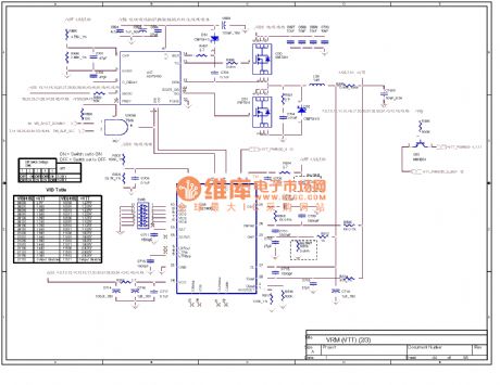
The computer mainboard circuit 830_42
Published:2011/7/20 8:11:00 Author:qqtang | Keyword: computer mainboard
View full Circuit Diagram | Comments | Reading(488)
The computer mainboard circuit 830_43
Published:2011/7/20 8:10:00 Author:qqtang | Keyword: computer mainboard
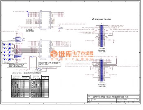
View full Circuit Diagram | Comments | Reading(515)
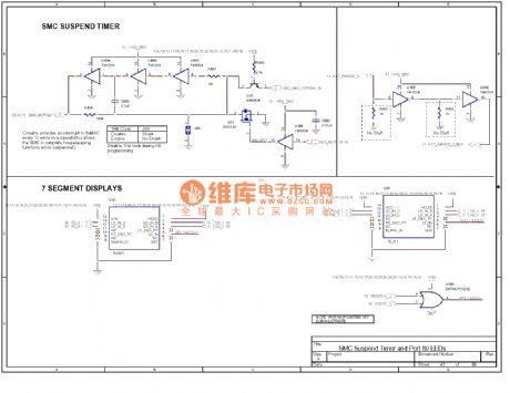
The computer mainboard circuit 830_44
Published:2011/7/20 8:09:00 Author:qqtang | Keyword: computer mainboard
View full Circuit Diagram | Comments | Reading(544)
The computer mainboard circuit 830_45
Published:2011/7/20 8:08:00 Author:qqtang | Keyword: computer mainboard
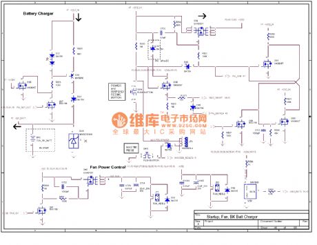
View full Circuit Diagram | Comments | Reading(521)
The computer mainboard circuit 830_46
Published:2011/7/20 8:07:00 Author:qqtang | Keyword: computer mainboard
View full Circuit Diagram | Comments | Reading(513)
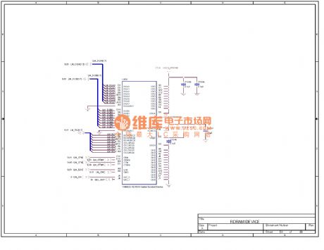
The computer mainboard circuit 830_47
Published:2011/7/20 8:06:00 Author:qqtang | Keyword: computer mainboard
View full Circuit Diagram | Comments | Reading(517)
The computer mainboard circuit 830-48
Published:2011/7/20 8:05:00 Author:qqtang | Keyword: computer mainboard
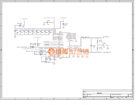
View full Circuit Diagram | Comments | Reading(556)
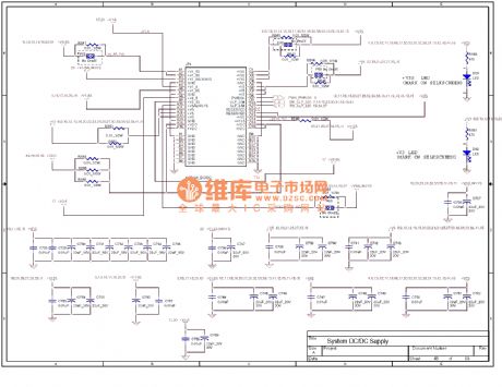
The computer mainboard circuit 830-49
Published:2011/7/20 8:04:00 Author:qqtang | Keyword: computer mainboard
View full Circuit Diagram | Comments | Reading(530)
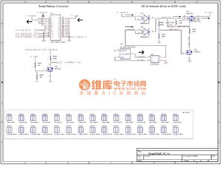
The computer mainboard circuit 830_41
Published:2011/7/20 8:12:00 Author:qqtang | Keyword: computer mainboard
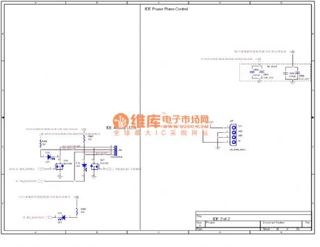
View full Circuit Diagram | Comments | Reading(570)
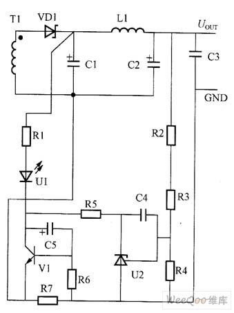
More precise constant voltage and constant current circuit composed of output voltage sag compensation function
Published:2011/7/20 0:41:00 Author:Fiona | Keyword: sag compensation function, constant voltage, constant current
The current mode working state:constant current control mode compares with the voltage drop of current sampling resistor R7 through setting the optocoupler LED's voltage drop.When the output current is not up to the constant current set point,the voltage drop of R7 reduces and it can be ignored;when the output current reaches the constant current point, C3 voltage drop of R7 increases,this increasing voltage converts the voltage into current and adds to the optocoupler's LED through the resistor R6 to make the current flowing through the LED increase, through the circuit's feedback GND control function,the output current is constant.
(View)
View full Circuit Diagram | Comments | Reading(599)
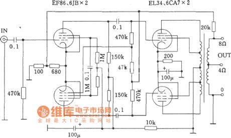
headphone amplifier composed of ECC822 tube circuit
Published:2011/7/14 23:12:00 Author:Fiona | Keyword: headphone amplifier, tube
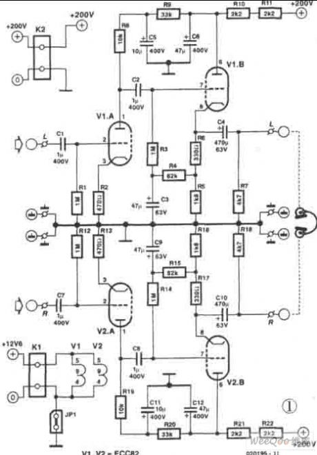
Pre-amplifier should generate sufficient signal amplitude to drive the headphones. The transistor part of pin 1,2,3 amplifies the signal. Input signal through the 50kΩ volume control logarithmic potentiometer P1 (P1 is not in Figure I) reaches the circuit board, and then inputs to the pre-amplifier stage directly through C1 and R1, and R1 and C1l provide the necessary negative gate bias. Gain is essentially determined by the R8. The maximum input voltage is determined by R2. R9 is so determined. That the current of the static anode chooses in the linear part of characteristic curve as possible.
(View)
View full Circuit Diagram | Comments | Reading(1238)
The hardware circuit of touch screen control chip ADS7843 and ColdFire processors
Published:2011/7/20 3:16:00 Author:Borg | Keyword: hardware circuit, touch screen control chip, ColdFire processors
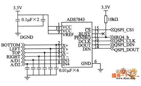
The hardware circuit of touch screen control chip ADS7843 and ColdFire processors is shown as above.
(View)
View full Circuit Diagram | Comments | Reading(874)
Operational Amplifier Basic Circuit
Published:2011/7/26 7:27:00 Author:Robert | Keyword: Operational, Amplifier, Basic
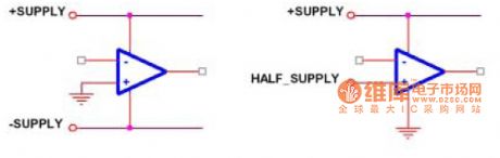
The positive power pin is connected to VCC+ and the ground or VCC- pin is connected to the GND. By taking a half of the positive voltage as virtual ground to connect to the operational amplifier's input pin, then the output voltage would be this virtual ground's voltage. And the operational amplifier's output voltage would take the virtual ground as center between the swing of Vom. There are some new operational amplifiers having two different maximum output voltage and minimum output voltage. This operational amplifier's data sheet would specifically point the Voh and Vol separately. It should be noted that many designers would use the virtual ground arbitrarily as reference for the input voltage and output voltage. But in most applications, the input and output use the power supply ground as reference. So the designers must add a DC-isolated capacitor in the input part and output part to isolate the DC voltage between the virtual ground and ground. (View)
View full Circuit Diagram | Comments | Reading(714)
LA7550 medium IC diagram
Published:2011/7/25 22:59:00 Author:Ecco | Keyword: medium IC
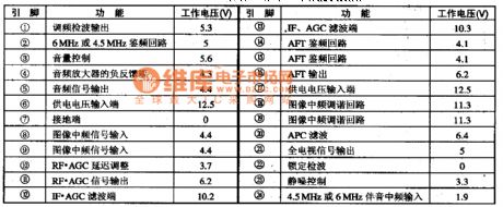
LA7550 medium IC produced by Sanyo is widely used in Hitachi series of large-screen TV, movement and the picture and sound IF signal amplification and processing in other domestic large-screen. 1. Features and functionsLA7550 IC contains the image and audio signal processing circuit, AGC control circuit, squelch control circuit, AFT automatic frequency control circuit. 2. pin functions and data LA7550 IC pin functions and data are listed in Table 1.
(View)
View full Circuit Diagram | Comments | Reading(787)
The field output circuit composed by discrete component
Published:2011/7/14 23:15:00 Author:Fiona | Keyword: field output circuit, discrete component

The field output circuit composed by OTL discrete component is widely used in a variety of brands machine(Usually used in 25 or below 25 inches machine), although the circuit bit numbers are not all the same, but the Circuit programs are selfsame,it can be referenced in repairs. (View)
View full Circuit Diagram | Comments | Reading(732)
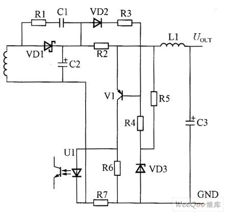
The circuit using NPN tube and voltage adjuster to realize the control of constant voltage and constant current
Published:2011/7/19 8:47:00 Author:Fiona | Keyword: NPN tube and voltage adjuster, constant voltage and constant current
The circuit using NPN tube and voltage adjuster to realize the control of constant voltage and constant current is shown as above:
(View)
View full Circuit Diagram | Comments | Reading(598)
Low-noise RF - IF amplifier circuit diagram
Published:2011/7/25 22:08:00 Author:Ecco | Keyword: Low-noise RF amplifier, IF amplifier
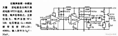
The circuit is composed of two 8FZ30 integrated circuits with wide frequency bandwidth, low noise. The main properties: voltage gain Gu = 40dB; bandwidth BW = 20 to 40MHz; input signal is 5μV to 50mV.
(View)
View full Circuit Diagram | Comments | Reading(1370)
MOSFET gate driver circuit
Published:2011/7/19 8:47:00 Author:Fiona | Keyword: MOSFET gate, driver
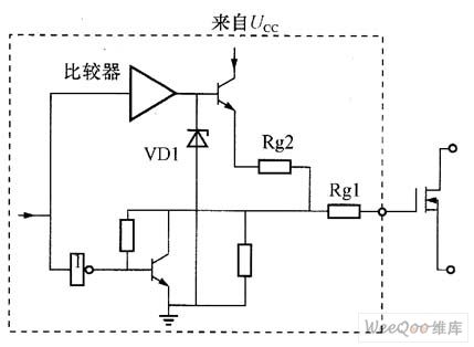
MOSFET driver circuit adds a regulator VD1 (UDRM = 8.3V) in the gate and gives the regulator a constant driving voltage,it can ensure MOOSFET always have a very good conduction. MOSEFT machine drive current is controlled by the Rg1 and Rg2,they can reduce the noise through controlling the MOSFET switching speed.When the MOSFET is off, the gate can be discharged through the resistor Rg1 to make the MOSFET quickly close and get the minimum switching loss,it is shown as above.
(View)
View full Circuit Diagram | Comments | Reading(1581)
Electron tube QUADll amplifier circuit diagram
Published:2011/7/25 22:11:00 Author:Ecco | Keyword: Electron tube amplifier
View full Circuit Diagram | Comments | Reading(763)
Wiring circuit diagram of operational amplifier application circuit input
Published:2011/7/16 9:44:00 Author:Sophia | Keyword: Operational amplifier application circuit input, Wiring
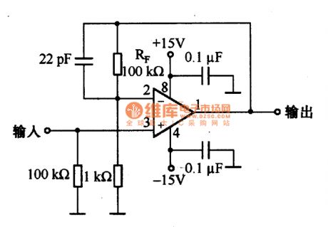
The wiring of op-amp applications circuit inputsThe impedance of Op amp's inverting input and the non-inverting inputare high, the input wiring should be short, otherwise, the external electrostatic and electromagnetic induction will generate noise. Figure is the in-phase amplifier circuit with phase gain of 40dB; the impedance of inverting input is high, if the wiring of this part is too long, which will lead to noise.So feedback resistor RF and Rs should be connected close to the inverting input to make the part of the high-impedance bea short connection. (View)
View full Circuit Diagram | Comments | Reading(933)
| Pages:172/250 At 20161162163164165166167168169170171172173174175176177178179180Under 20 |
Circuit Categories
power supply circuit
Amplifier Circuit
Basic Circuit
LED and Light Circuit
Sensor Circuit
Signal Processing
Electrical Equipment Circuit
Control Circuit
Remote Control Circuit
A/D-D/A Converter Circuit
Audio Circuit
Measuring and Test Circuit
Communication Circuit
Computer-Related Circuit
555 Circuit
Automotive Circuit
Repairing Circuit