
Index 178
TDA7496 two-channel audio power amplifier integrated circuit diagram
Published:2011/5/17 4:10:00 Author:Ecco | Keyword: two-channel , audio , power amplifier , integrated circuit
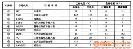
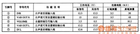
TDA7496 is the two-channel audio power amplifier IC produced by Philips, it is widely used in the high-fidelity audio, car audio, multimedia and so on. 1. Features of functionTDA7496 integrated circuit contains two audio power amplifier circuits with the same functions, and it has electronic volume control circuit, the squelch control circuit, overheat protection and short circuit protection, mono output power is 6W, limit working voltage is 30V. 2. Pin functions and data TDA7496 IC uses 15-pin single in-line package, the pin functions and data are listed in Table 1. Table 1 shows TDA7496 integrated circuit pin functions and data.
(View)
View full Circuit Diagram | Comments | Reading(1563)
TDA7495 two-track audio power amplifier integrated circuit diagram
Published:2011/5/17 4:10:00 Author:Ecco | Keyword: two-track , audio, power amplifier, integrated circuit
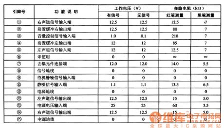
TDA7495 is the two-channel audio power amplifier integrated circuit produced by Philips, it is widely used in home hi-fi, television, stereo, car audio and multimedia audio. 1. The featuresand functionsTDA7495 integrated circuit contains two audio power amplifier circuits with the same features, and it also has two independent mute function with thermal overload protection and short circuit protection, and output power is 20W. 2. Pin functions and data TDA7495 IC uses 15-pin single in-line package, the pin functions and data are listed in Table 1. Table 1 shows TDA7495 integrated circuit pin functions and data.
(View)
View full Circuit Diagram | Comments | Reading(966)
TDA7298 high-fidelity AB audio power amplifier IC diagram
Published:2011/5/17 4:10:00 Author:Ecco | Keyword: high-fidelity , AB , audio power, amplifier, IC
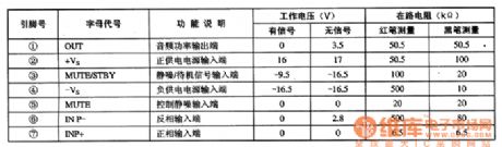
TDA7298 is high-fidelity AB audio power amplifier IC produced by SGS in Europe, it is widely used in high-Rover, TCL, and other large-screen color TV. 1.The featuresand functionsTDA7298 integrated circuit is primarily composed of power amplifier, mute / standby control circuit, over current and short circuit protection circuit. When Vcc = ± 22V, RL = 4Ω, RL = 8Ω, the output power can reach 28W. 2. Pin functions and data TDA7298 IC uses the package with 7 pin in single row, the pin functions and data are listed in Table 1.Table 1 shows TDA7298 integrated circuit pin functions and data
(View)
View full Circuit Diagram | Comments | Reading(1295)
CL328-6-Communication signal chip microcomputer integrated circuit
Published:2011/7/13 4:38:00 Author:leo | Keyword: Signal chip, communication
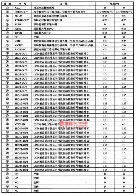
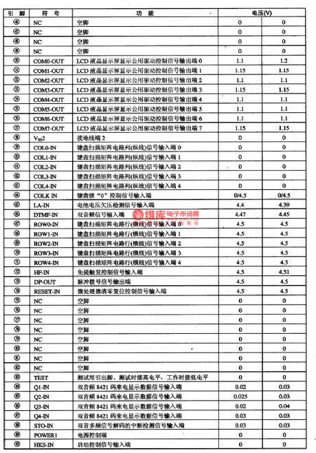
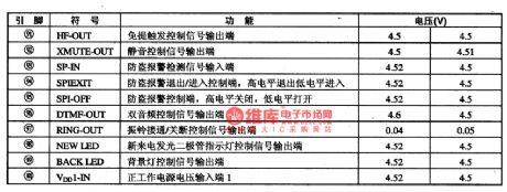
CL328-6 is communication signal chip microcomputer integrated circuit which is widely used in caller ID telephone.1.Function features:CL328-6 contains dual audio signal generator circuit, theft deterrent telephone, pulse signal generator circuit, caller ID decoding circuit, battery under voltage test circuit, ringing test circuit, display drive circuit, key switch RoHS code circuit and others. 2.Pin functions and data:It uses 100-pin soft package and the pin functions as well as related information are shown in the picture 1. (View)
View full Circuit Diagram | Comments | Reading(846)
Electric bridge sensing isolated amplifier circuit diagram
Published:2011/7/1 3:16:00 Author:Rebekka | Keyword: Electric bridge, sensing isolated amplifier
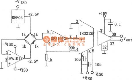
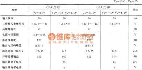
Many sensors, such as the strain gauge platinic resistance, pressure sensor, the gas detection, etc. They use the electric bridge as sampling circuit differential signal. The figure shows the circuit using a single power supply high precision double luck OPA1013 as preamplifier. It uses the double mouth isolation miniaturization isolated amplifier ISO212P as level after isolated amplifier.
(View)
View full Circuit Diagram | Comments | Reading(938)
TRF5O01 GPS RF receiving and collecting integrated circuit
Published:2011/7/13 20:07:00 Author:leo | Keyword: GPS, RF, Integrated circuit
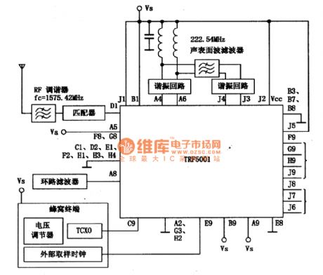
TRF5O01 is a type of GPS RF receiving and collecting integrated circuit used in GPS positioning system.
Function features:
TRF5O01 has the cellular terminal and emitter with sources. It contains low noise amplifier mixer. The first and second LO set-frequency synthesizer and four bit ADC and so on are always used in high sensibility GPS system. TRF5O01 working voltage is 2.7 V to 3.3 Vand the current consumption is super light. When the voltage is 2.7 V, its current consumption is 49 mA. (View)
View full Circuit Diagram | Comments | Reading(984)
LAG665-The single chip stereophonic reproduction integrated circuit
Published:2011/7/13 20:12:00 Author:leo | Keyword: Single chip, Stereophonic reproduction, Integrated circuit
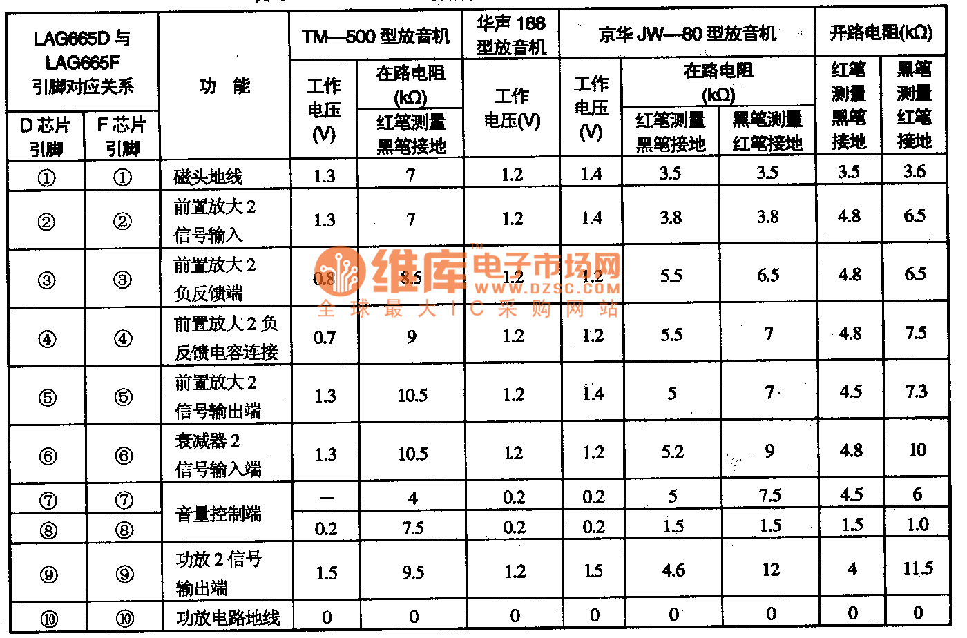
 LAG665 is the third generation single chip personal stereo stereophonic reproduction integrated circuit. It has multiple function and made by MITSVMI.
Inner circuit function:LAG665 has a dual channel front magnetic head amplifier, backward stage earphone drive, double power amplifier and electronic DC volume control function and so on.
Package construction: It has two kinds of package construction. LAG665D adopts 30 pin dual line package. And LAG665F uses 28 pin package construction. They have the same electrical property and inner diagram. (View)
LAG665 is the third generation single chip personal stereo stereophonic reproduction integrated circuit. It has multiple function and made by MITSVMI.
Inner circuit function:LAG665 has a dual channel front magnetic head amplifier, backward stage earphone drive, double power amplifier and electronic DC volume control function and so on.
Package construction: It has two kinds of package construction. LAG665D adopts 30 pin dual line package. And LAG665F uses 28 pin package construction. They have the same electrical property and inner diagram. (View)
View full Circuit Diagram | Comments | Reading(2318)
The rotate speed test circuit made by optoelectronic transistor
Published:2011/7/13 20:10:00 Author:leo | Keyword: Rotate speed test circuit, Optoelectronic transistor
The picture1 shows rotate speed test circuit made by optoelectronic transistor and so on. When the luminous flux of the optoelectronic transistor VT1 increases by 1%, photo current generates 500 mV voltage between VT2 and VT3. And this voltage is stable logarithm relation under the biggish photoelectic current.Therefore, this circuit can work normally however the optical line changes. A1 and related components form high gain self-adapting filter which can hold down the photo noise in the environment and add clean signals to comparator and input port. (View)
View full Circuit Diagram | Comments | Reading(1028)
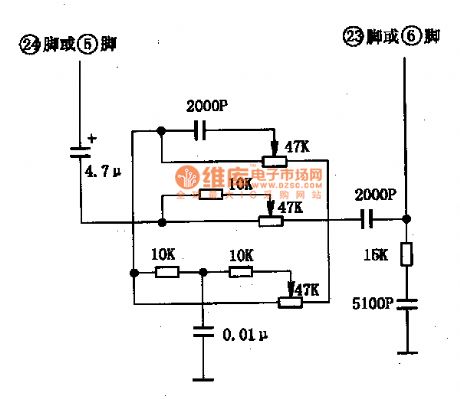
Single-supply inverting amplifier circuit composed of the μA709
Published:2011/6/27 20:15:00 Author:Rebekka | Keyword: Single-supply inverting amplifier
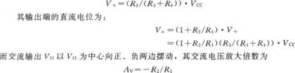
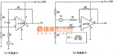
(a),(b)。(a)、(b),R3、R4,:
(View)
View full Circuit Diagram | Comments | Reading(792)
LA4520-Single chip playback integrated circuit
Published:2011/7/13 20:09:00 Author:leo | Keyword: Single chip, playback
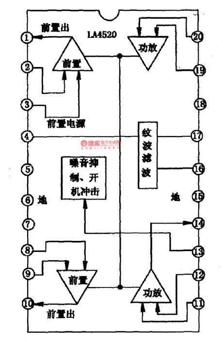
LA4520 is a single chip playback integrated circuit produced by Sanyo Company in Japan, which is widely used in all kinds of playersand recording playback devices. 1. LA4520 inner circuit diagram and pin functions:LA4533M contains two similar fronted power amplifiers, and stereo system circuit. It uses 20-pin dual-line package. The inner circuit diagram of LA4520 is shown in the picture 1-1.2. LA4520 classic applying circuit is shown in the picture 1-2.3. Signal processPicture 1-3 gives the whole process of the play signals. (View)
View full Circuit Diagram | Comments | Reading(1854)
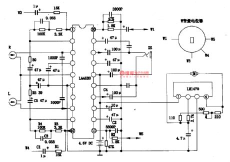
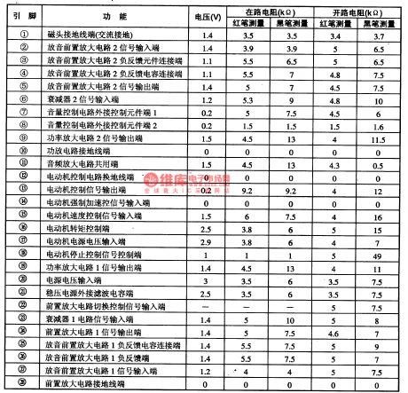
CXA1034P-Single chip stereo integrated circuit
Published:2011/7/13 4:40:00 Author:leo | Keyword: Single chip, stereo
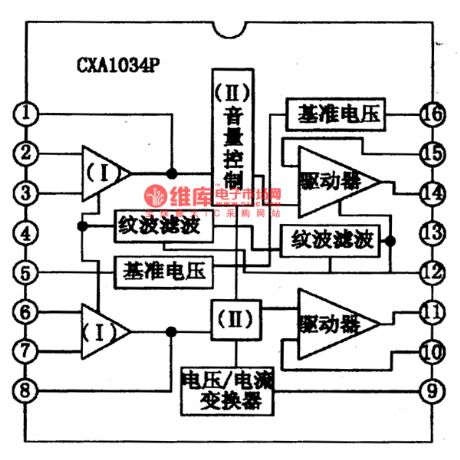
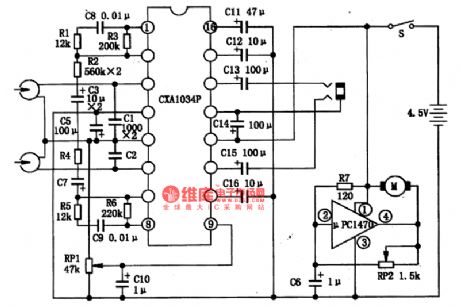
CXA1034P is a single chip playback integrated circuit produced by Sanyo Company in Japan which is widely used in all kinds of low voltage recorders. 1. CXA1034P inner circuit diagram and pin functions:CXA1034P contains two similar fronted power amplifiers, two power amplifiers, less outer components, and single electric voltage controlling stereo volume controller. It uses 16-pin dual-line package. The inner circuit diagram of CXA1034P is shown in the picture 1.2. CXA1034P classic applying circuit is shown in the picture 2.CXA1034P’s power supply voltage is from 1.8 B to 10 V. (View)
View full Circuit Diagram | Comments | Reading(1949)
KA22135-Single chip stereo player integrated circuit
Published:2011/7/13 4:40:00 Author:leo | Keyword: Single chip, stereo player
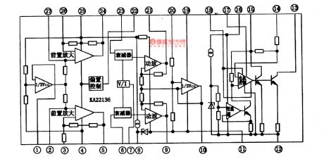
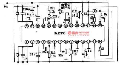
KA22135 is single chip stereo player integrated circuit produced by Samsung in Korea. 1.KA22135 inner circuit diagram and pin functions:KA22135 contains two fronted amplifiers, double power amplifier and electric DC volume control circuit and DC device speed regulator circuit.It has two packages. KA22136F is 28-pin dual line package and KA22136 is 28-pin dual-line flat package. They have the same inner functions and the inner circuit diagram is shown in the picture 1-1.2.KA22135 main parameters:Its work voltage converge is from 2.1 V to 5 V and the classic work voltage is 3 V. When Vcc is 3 V and RL is 32, its output power is 28 mW x 2.3.KA22135 classic applying circuitIts classic applying circuit is shown in the picture 1-2. (View)
View full Circuit Diagram | Comments | Reading(1657)
KA22134-Single chip stereo player integrated circuit
Published:2011/7/13 4:39:00 Author:leo | Keyword: Single chip, stereo player
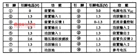
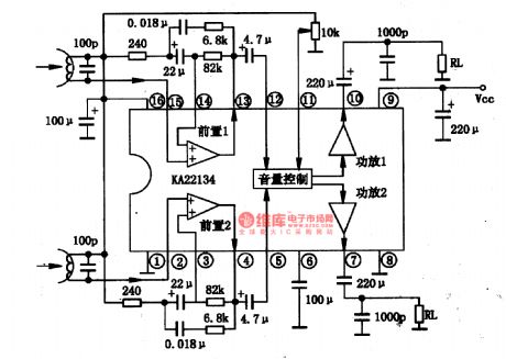
KA22134 is single chip stereo player integrated circuit produced by Samsung in Korea which is used in the low voltage walkman. 1.KA22134 inner circuit diagram and pin functions:KA2214 contains two fronted amplifiers, double power amplifier and electric DC volume control circuit and DC device speed regulator circuit.It uses 16-pin dual line package and the inner circuit diagram is shown in the picture 1-1.2.KA22134 main parameters:Its work voltage converge is from 1.8 V to 6 V and the classic work voltage is 3 V. (1)Maximum output voltage of fronted amplifier Vom. When THDI is 10%, its value is 770mV. (2)The output power of driver Po. When THD2 is 10%, its classic value is 30 dB. (View)
View full Circuit Diagram | Comments | Reading(1972)
KA22131-Single chip stereo player integrated circuit
Published:2011/7/13 4:39:00 Author:leo | Keyword: Single chip, stereo player
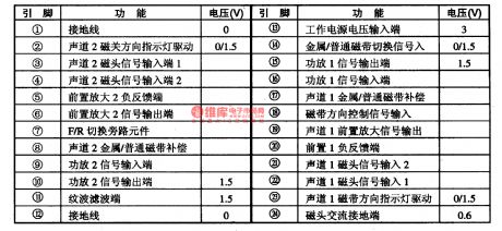
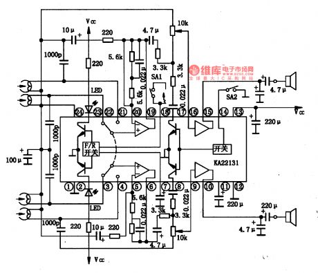
KA22131 is single chip stereo player integrated circuit produced by Samsung in Korea which is used in the low voltage stereo system. 1.KA22134 inner circuit diagram and pin functions:KA2214 contains two fronted balance amplifiers, power amplifier and cassette type selecting circuit and others. It uses 24-pin dual line flat package and the inner circuit diagram is shown in the picture 1-1.2.KA22134 main parameters:Its work voltage converge is from 1.8 V to 3.6 V and the classic work voltage is 3 V. When Vcc is 3 V and RL is 16 ohms, the Po is 69mW x 2.
(View)
View full Circuit Diagram | Comments | Reading(1767)
The circuit diagram of a power MOSFET amplifier circuit with high frequency feature
Published:2011/7/13 19:49:00 Author:leo | Keyword: Power MOSFET amplifier, high frequency
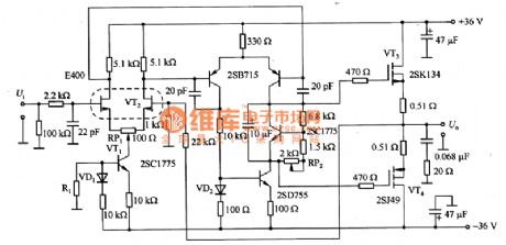
The picture 1 is a power MOSFET amplifier circuit with high frequency feature. In order to restrain the influence of the changes of power supply, it takes VT1 and VT2 to form the constant current circuit,while, VT3 and VT4 are end power amplifying circuit. Due to the influence of offset current, its drain currenthastemperature factors which is from positive to negative. Therefore, it uses RP2 to control the offset in order to set the drain current to 0.1 to 0.2 A, which passes through VT3 and VT4. And when its frequency is 1Hz to 800 kHz, the distortion is 0.04% per 1 kHz. At the same time, its output power is 40 W and the convert rate is 100V/μs. (View)
View full Circuit Diagram | Comments | Reading(2746)
The circuit diagram of a high frequency bias magnetic amplifier used by earphones
Published:2011/7/13 19:50:00 Author:leo | Keyword: Bias magnetic amplifier, high frequency

The picture 1 shows a high frequency bias magnetic amplifier used by earphones. Its resistance is 30 to 100 Ω, so it takes TC28 as the driver to meet the need, whose resistance is 6Ω. In TC28, four simple negaterG1 to G4 make up of a full bridge circuit. This bridge circuit is used to drive the left and right audio channel of the earphones. TL451 is the integrated controller of switch power resourcing. During simulating, if the left and right audio channels output signals with different frequency, the frequency difference will be added to output signals as the deadbeat signals. (View)
View full Circuit Diagram | Comments | Reading(1074)
A differential test circuit made by analog switch
Published:2011/7/13 19:55:00 Author:leo | Keyword: Test circuit, Analog switch

What the picture shows is a differential test circuit made by analog switch. In the circuit, sensor uses hall component H. When magnetic field is imposed vertically on hall component H, the control current value between a and b is l1, then the hall voltage produced is KBI1 plus UB. In this formula UH=KBI1+UB, k is the proportionality constant, UB is unbalanced voltage. In order to clear this unbalanced voltage, we can make the average of the control current I1 of this hall component equal to zero. We can do this by using switch s10 and s20 to convert the control current I1 alternately to make the amplitude of vibration equal to the time at the moment. At the same time, to make the hall component have a steady sensibility, we only need to make the control current I1 steady. Control current is decided by Ur and Rs, that is I1=Ur/Rs. (View)
View full Circuit Diagram | Comments | Reading(852)
A simple transistor test circuit
Published:2011/7/13 19:55:00 Author:leo | Keyword: Simple transistor test circuit, P channel FET
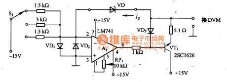
As the picture a and b show, it is a simple transistor test circuit. The picture13(a) shows a FET test circuit. This circuit is mainly used to test FET pinch-off voltage UP and grid-source voltage UGS. In the circuit, VT is the FET to be tested, and A1 can form servo circuit whose output controls reversal phase input terminal potential and makes it become zero. Voltage-stabilizing diode VD3 and VD4 can produce voltage of±9V and clamp-on the grid potential of VT. R5 is the current limiting resistance which controls VT grid potential current and makes it under the set value. When S2 is connected to 1, VT grid potential voltage is higher than clamp-on voltage and A1 output is negative to the N channel FET while positive to the P channel FET. (View)
View full Circuit Diagram | Comments | Reading(1455)
ULN3839A-An AM single chip audio integrated circuit
Published:2011/7/13 19:56:00 Author:leo | Keyword: Single chip audio integrated circuit, Pocket-sized radio
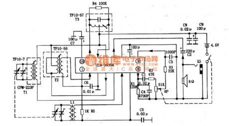
ULN3839A is a kind of single chip audio integrated circuit used in pocket-sized radio and other kinds of radios.
1.ULN3839A integrated chip inner circuit diagram and pin functions:ULN3814A has three suffix: ULN3839A-1, ULN3839A-2 and ULN3839A-3. These three kinds of circuit are almost the same. ULN3839A has all AM audio circuits including AM AGC, LO, MIX, ZF, detection and so on. It adopts 16 pins direct inserting package which you can see in the picture.
2.Main parameters of ULN3839A:Its power supply voltage is 1.8 V to 10 V and the classic operating voltage is 3 V , 4.5 V and 6 V. When Vcc is 3 V and Ta is 25℃, it has the following parameters:(1)Sensibility S. When Vo is 20 mV , its classic value is 3μV(2)Detection output. Its classic value is 100 mV.(3)Voltage gainG(V). Its minimum value is 36 dB and maximum value is 44 dB and classic value is 40 dB.(4)Output power Po. When D is 10%,When Vcc is 3 V, its classic value is 50 mW;When Vcc is 6 V, its minimum value is 250 mW and classic value is 350 mW. (View)
View full Circuit Diagram | Comments | Reading(1576)
Chopper amplifer circuit made by TA7505
Published:2011/7/13 19:39:00 Author:leo | Keyword: Chopper, amplifer circuit
Picture 1 is a chopper amplifier made by TA7505, which contains a chopper circuit, synchronous rectifying and modulating circuit. The switch component of chopper and synchronous rectifier mainly adopts FET tube, such as VT1 (3SK38) in picture 1(a). This tube is a kind of FET tube which changes to stop state when the voltage is 3V(the maximum value). VT5 and VT6 can make up of multivibrator circuit which can generate the square wave voltage. The square wave voltage passes the trigger made by VT3 and VT4 to adjust the wave shape, after which the signals come to modulate the VT1 grid. (View)
View full Circuit Diagram | Comments | Reading(2086)
| Pages:178/250 At 20161162163164165166167168169170171172173174175176177178179180Under 20 |
Circuit Categories
power supply circuit
Amplifier Circuit
Basic Circuit
LED and Light Circuit
Sensor Circuit
Signal Processing
Electrical Equipment Circuit
Control Circuit
Remote Control Circuit
A/D-D/A Converter Circuit
Audio Circuit
Measuring and Test Circuit
Communication Circuit
Computer-Related Circuit
555 Circuit
Automotive Circuit
Repairing Circuit