
Index 163
45_MHz_SOUND_IF_AMPLIFIER
Published:2009/6/19 4:34:00 Author:May
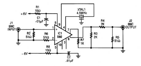
An NE592 is used as a 4.5-MHz amplifier sound subcarrier in video applications. XTAL1 is a 4.5-MHz crystal or ceramic resonator. (View)
View full Circuit Diagram | Comments | Reading(5018)
GENERAL_PURPOSE_OUTPUT_AMPLIFIER
Published:2009/6/19 4:33:00 Author:May
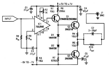
This general-purpose amplifier has a bandwidth of approximately 20 MHz and it uses an LM733/NE592 video amp IC. This circuit can be used as a line driver or as a LAN line driver. (View)
View full Circuit Diagram | Comments | Reading(5941)
LOW_NOISE_INSTRUMENTATION_AMPLIFIER
Published:2009/6/19 4:33:00 Author:May
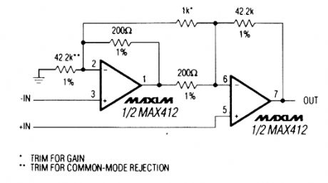
A Maxim MAX412 IC amplifier is used in this circuit. The supply current is ±5 V at 5 mA. (View)
View full Circuit Diagram | Comments | Reading(1079)
ac_COUPLED_INSTRUMENTATION_AMPLIFIER
Published:2009/6/19 4:32:00 Author:May
View full Circuit Diagram | Comments | Reading(679)
HIGH_INPUT_IMPEDANCE_INSTRUMENTATION_AMPLIFIER
Published:2009/6/19 4:31:00 Author:May

View full Circuit Diagram | Comments | Reading(1274)
DIFFERENTIAL_NPUT_INSTRUMENTATION_AMPLIFIER
Published:2009/6/19 4:30:00 Author:May
View full Circuit Diagram | Comments | Reading(597)
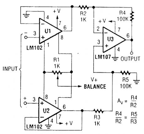
PROGRAMMABLE_GAIN_INSTRUMENTATION_AMPLIFIER
Published:2009/6/19 4:29:00 Author:May
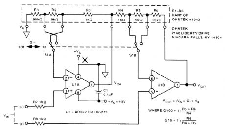
This is a two-op-amp programmable-gain instrumentation amplifier for single-supply applications. U1A and U1B are Analog Devices AD822 or OP-213 ICs. (View)
View full Circuit Diagram | Comments | Reading(688)
VARIABLE_GAIN_DIFFERENTIAL_INPUT_INSTRUMENTATION_AMPLIFIER
Published:2009/6/19 4:28:00 Author:May
View full Circuit Diagram | Comments | Reading(1158)
1INSTRUMENTATION_AMPLIFIER
Published:2009/6/19 4:26:00 Author:May
View full Circuit Diagram | Comments | Reading(735)
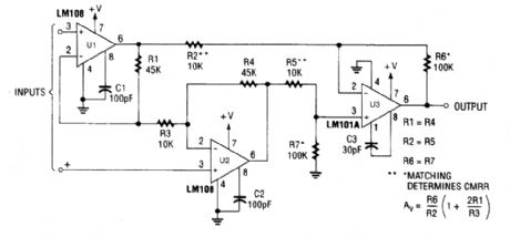
×100INSTRUMENTATION_AMPLIFIER
Published:2009/6/19 4:26:00 Author:May
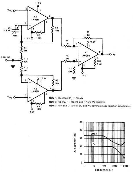
CMRR vs.frequency. (View)
View full Circuit Diagram | Comments | Reading(621)
Quasi-digital amplifier circuit diagram
Published:2011/6/27 1:25:00 Author:Rebekka | Keyword: Quasi-digital amplifier
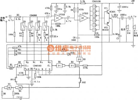
Quasi-digital amplifier. Its power amplification process uses digital means (PWM), and the volume control also is digital. The Sl ~ S4 in the CMOS analog switch CD4066 and the composition of binary reversible counter CD40193 form the digital volume control circuit. Press ANl key, 2Hz clock pulse from the NAND gate H3, H4, and the output of NAND gate H2 turn into CD40193 of CL + side and the CD40193 is counted by addition; When you press AN2 key, the clock pulse of the non-2Hz Gate Bl, B2 enters the CL-end CD40193. The CD40193 is counted by subtraction. (View)
View full Circuit Diagram | Comments | Reading(2010)
High-precision pressure amplifier circuit composed of the AD624
Published:2011/6/27 0:12:00 Author:Rebekka | Keyword: High-precision pressure amplifier
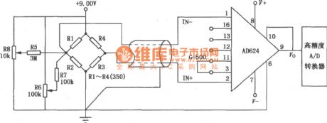
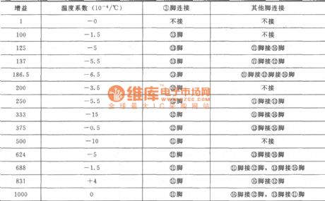
High-precision pressure amplifier circuit is mainly used in small amplification system. The AD624 is a precision low-noise instrumentation amplifier which can be used in a small sensor output signal amplification system. The figure shows the high-precision pressure amplifier circuit composed of the AD624. The sensor is a standard strain gauge bridge sensors. The bridge voltage uses+ 9.00V, potentiometers R8 and R6 to zero, in which R6 is coarse, R8 is fine. The amplifier output can be directly related to high-precision A / D converter connected. (View)
View full Circuit Diagram | Comments | Reading(1815)
ECG_AMPLIFIER_WITH_RIGHT_LEG_DRIVE
Published:2009/6/19 4:19:00 Author:May
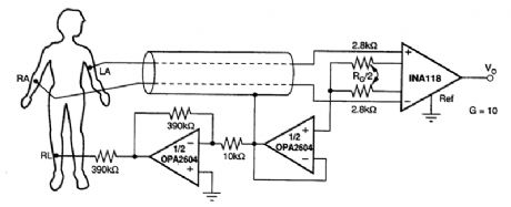
View full Circuit Diagram | Comments | Reading(2217)
High-precision measurement amplifier circuit composed of the INA131
Published:2011/6/27 1:51:00 Author:Rebekka | Keyword: High-precision measurement amplifier
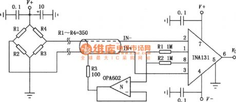
The INA131 is a low-cost general-purpose amplifier. Its inside gain resistor passes laser trimmed and makes the gain error small. It provides a standard gain of 100. The figure shows the high-precision measuring amplifier and the input signal of the electrical diagram bridge sensor (load cell, such as strain, displacement measurement sensors, etc.). This connection of the 50Hz power interference and high common mode interference rejection is very high. The magnification is 100, if you need a higher gain, you can add a gain resistor RG in ①, ⑧ foot indirectly. The gain size: G = 100 +250 kΩ / RG. (View)
View full Circuit Diagram | Comments | Reading(1194)
Operational amplifier all-function zero method circuit diagram
Published:2011/6/27 4:53:00 Author:Rebekka | Keyword: Operational amplifier all-function zero method
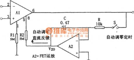
The figure shows the generic auto-zero circuit. A2 is the FET input type integrated chip. The integrator is composed of R, C, etc. It can be integrated to the DC output offset voltage. The switch S is an electronic switch that can automatically achieve the sampling time period. It can make the A1 output offset voltage be used as the input signal. The output points drive the zero end of A1, so that the offset voltage is the minimum state . The resistance of resistors R1 and R2 are larger. The different types of integrated operational amplifier values is around 5MΩ. (View)
View full Circuit Diagram | Comments | Reading(616)
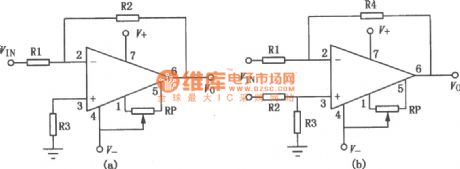
Op amp application input end zeroing circuit diagram 1
Published:2011/5/16 21:52:00 Author:Rebekka | Keyword: Op amp application , input end zeroing

Figure (a) is a relatively simple circuit. It uses the input resistors R1 and the feedback resistor R2 as a part of the attenuation network. It generates a variable offset voltage with resistor R3 at the inverting input end. The voltage of the circuit is divided by R3 and R1,R2. The 2 ends of the potentiometer R4 connect with ± 15V power supply. The partial pressure ratio is about 1000 / 1. It can get ± 15mV offset voltage range. In figure (a), the general formula of the offset voltage adjustment range is:
Offset voltage range = ± VD · [(R1 ∥ R2) / R3] (± VD = ± 15V)
When there are multiple input signals at the reverse side. It is shown in figure (a) by the virtual display line. Its offset voltage range: Multiple input offset voltage range = ± VD [(R1 ∥ R2 ∥ Rl ') / R3] (± VD = ± l5V).
The circuit shown in figure (b) has a large application value. Since the adjusting voltage has no relationship with the feedback components, while the adjusting voltage is applied to the phase input terminal and avoid the winning stream signaling pathways. In this circuit, the resistance value of R3 and R5(100kΩ, 100Ω) form the 1000 / I voltage dividing circuit. The 2 terminals of R5 get ± 15mV offset voltage adjustment range. When the values of R3, R5 change. The offset voltage adjustment range is determined by:
Offset voltage adjustment range = ± VD · (R5/R3) (± VD = ± l5V) (View)
View full Circuit Diagram | Comments | Reading(599)
Photodiode isolation amplifier circuit diagram composed of ISO212P
Published:2011/6/26 22:06:00 Author:Rebekka | Keyword: Photodiode isolation , amplifier circuit
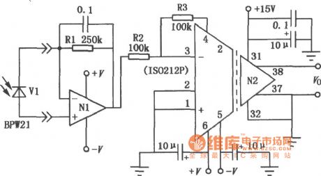
Photodiode isolation amplification circuit uses the photodiode to provide a reliable power supply isolation between the signal path and the two channels of the power supply. IS0212P is a low-cost miniaturized transformer-coupled isolation amplifier circuit. The chip uses two high-efficiency small toroidal transformer and provide reliable isolation between the signal path and the two channels of the power supply. Figure shows the typical application of IS0212P in optical detection, the photodiode is added to the two inputs of BPW21 and OPAl28 (N1) and forms the I / U resistor gain, it uses a larger feedback resistor. (View)
View full Circuit Diagram | Comments | Reading(1534)
The offset zeroing circuit of differential amplifier
Published:2011/5/12 5:08:00 Author:Rebekka | Keyword: differential amplifier, offset zeroing

The offset zeroing circuit of differential amplifier is shown as above. When you lead the offset adjusting voltage to the differential amplifier circuit, it should not affect the balance of differential mode signal. In the circuit high-voltage divider ratio composed of R3 and R5. It provides variable potential to the right end of R2. Then it is passes R1 and R2 partial pressure. It gains the offset adjusting voltage at the inverting input of op amp. Generally the value of resistance R5 is small, its purpose is to raise partial pressure ratio. In order to obtain a high accuracy, sometimes in order to reduce the introduction of the common mode error, you need to adjust R2' to achieve the purpose.
R2/R1=(R2'+R5)/R1'
The circuit is shown in Fig. Its offset adjust voltage range determined by the following:Offset voltage range = VD (R5 / (R3 + R5)) (R1 '/ R1' + R2 ')Based on the data graph, the offset adjustment range is ± 15mV. (View)
View full Circuit Diagram | Comments | Reading(835)
Precision electric bridge isolation amplifier circuit composed of ISO100
Published:2011/6/26 22:16:00 Author:Rebekka | Keyword: Precision electric bridge , isolation amplifier
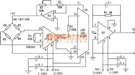
The precision electric bridge isolation amplifier circuit composed of ISO100 is mainly used for weighing, pressure measurement systems. ISO100 is a small, inexpensive optical isolation amplifier, the internal LED light passes the excitation and the optical receiver tube receives transmission. Figure shows the the main applications of the precision electric bridge isolation amplifier circuit. The bridge outputs 0 ~-l0mV unipolar signal. It is firstly amplified for 100 times by INA101 precision instrumentation amplifier, and then sent through the 100kΩ resistor Rl unipolar input ISO100 to ensure linear operation of the ISO100. (View)
View full Circuit Diagram | Comments | Reading(1025)
CFl55 Series dual power high input impedance single op amp circuit diagram
Published:2011/5/15 6:16:00 Author:Rebekka | Keyword: dual power , high input impedance , single op amp
The input circuit of CFl55 series op-amp is composed of the FET. The features are: It has a very small input current, low supply current, low power consumption, low noise, its offset voltage is small, peripheral-zero side. The series can be used for high-speed integrators, the sample and keeping circuit of fast D / A converter etc. Its similar or direct substitution models are: CFl55MT, CF255LT, CF355CT, CFl55MD, CF255LD, CF355CD, CFl55MJ, CF255LJ, CF355CJ, CF355CP and so on. The CFl55 typical application circuit is shown as above. Figure (a) is the inverting amplifier and the zeroing circuit. Figure (b) is the differential input and zeroing circuit. (View)
View full Circuit Diagram | Comments | Reading(505)
| Pages:163/250 At 20161162163164165166167168169170171172173174175176177178179180Under 20 |
Circuit Categories
power supply circuit
Amplifier Circuit
Basic Circuit
LED and Light Circuit
Sensor Circuit
Signal Processing
Electrical Equipment Circuit
Control Circuit
Remote Control Circuit
A/D-D/A Converter Circuit
Audio Circuit
Measuring and Test Circuit
Communication Circuit
Computer-Related Circuit
555 Circuit
Automotive Circuit
Repairing Circuit