
Index 171
SERIES_PARALLEL_LOOP_ALARM
Published:2009/6/14 21:38:00 Author:jailer
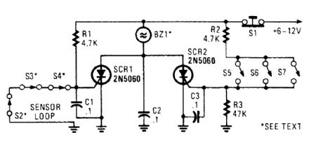
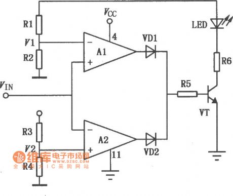
Two SCRs are used with two sensor loops. One loop uses series switches, the other loop parallel switches. When a switch actuation occurs, the SCR triggers. The alarm should be a noninterrupting type. (View)
View full Circuit Diagram | Comments | Reading(893)
MULTI_LOOP_PARALLEL_ALARM
Published:2009/6/14 21:35:00 Author:jailer
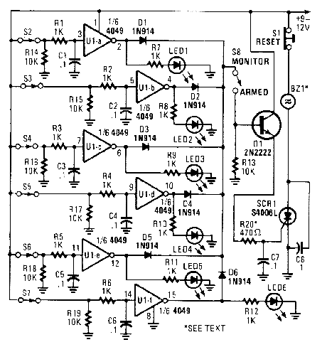
This alarm has status LEDs connected across each inverter output to indicate the status of its as-sociated sensor. S8 is used to monitor the switches via the LEDs, or to trigger an alarm via Q1 and SCR1. BZ1 should be a suitable alarm of the noninterrupting type. (View)
View full Circuit Diagram | Comments | Reading(799)
HIGH_POWER_ALARM_DRIVER
Published:2009/6/14 21:32:00 Author:jailer
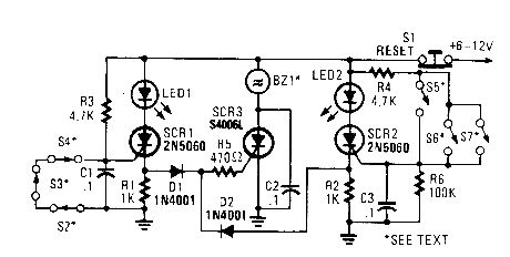
In this circuit, a low-powered SCR is used to trigger a higher powered SCR. When a switch is opening (52, 53, 54) or closing (55, 56, 57), ei-ther SCR1 or SCR2 triggers. This triggers SCR3 via Dl, D2, and R5. BZ1 is a high-powered alarm of the noninterrupting type. (View)
View full Circuit Diagram | Comments | Reading(852)
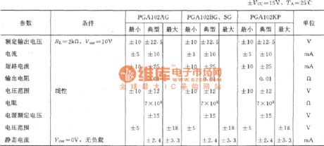
Data gain high speed cascade amplifier circuit composed of the PGA102
Published:2011/6/30 10:31:00 Author:Rebekka | Keyword: Data gain high speed , cascade amplifier
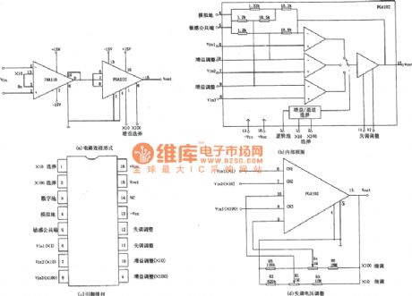
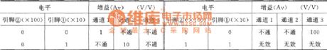
The the relationship of the gain value and control the level:
The main parameters of the integrated chip's PGA102:
The figure shows the data gain high speed cascade amplifying circuit. This circuit is composed of the umerical control instrument amplifier INA110 and the gain programmable integrated op-amp PGA102. When the 3 pin of the INAll0 connects with the pins 13, the voltage amplifier multiples is Av = 10. The control of the gain circuit is compeleted by the first level 2 PGA102 integrated op-amp.
(View)
View full Circuit Diagram | Comments | Reading(583)
The gain automatic controllable shift amplifier circuit composed of PGA202
Published:2011/6/30 10:20:00 Author:Rebekka | Keyword: gain automatic, controllable shift amplifier
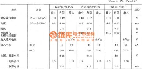
The figure shows the automatic gain control shift amplifier circuit. This circuit consists of four parts: The amplification unit circuit gain programmable instrument (with amplification integrated chips PGA202 component). It adds and subtracts counter unit, two-way comparator unit and 10 V benchmark voltage source. The internal structure of PGA202 is shown in figure (b), its gain can be controlled by TTL level, the integrated chips and single-chip microcomputer are easily interfaced. The PGA202 for mosfet input type and includes the conductive road, it can realize across the bandwidth in different gain almost the same. (View)
View full Circuit Diagram | Comments | Reading(554)
High input impedance three op amp differential amplifier circuit diagram
Published:2011/6/27 4:59:00 Author:Rebekka | Keyword: High input impedance, three op amp differential amplifier
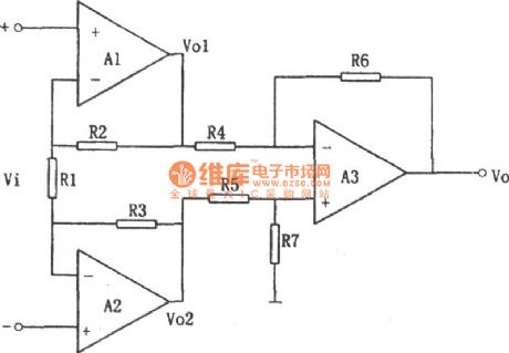
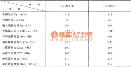
The circuit is mainly used for the monitor the signal pre-amplification or amplification of various data, which is sometimes referred to be used as data amplifier circuit. Figure shows a four-op-amp OP-09A integrated chip. In order to increase input impedance. It still uses the same phase of adding signal voltage input method. In order to ensure the two sources are added to the op amp's inverting input. It uses the two-phase amplifier A1 and A2 to form the first stage amplifier. Table 1 shows the OP-09A quad op amp integrated amplifier electrical characteristics table. (View)
View full Circuit Diagram | Comments | Reading(937)
Switching gain amplifier circuit composed of the INA115
Published:2011/6/27 4:20:00 Author:Rebekka | Keyword: Switching gain amplifier
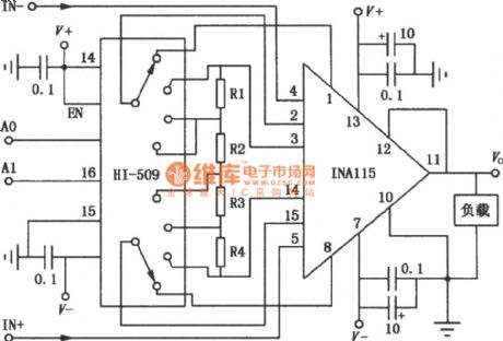
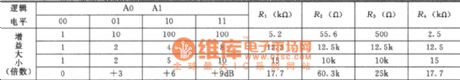
Switching gain amplifier circuit composed of the INA115 provides a different gain, it is shown as above. The lNA115 is a low cost general instrumentation amplifier, the circuit does not require external imbalance . It can be obtained a very high accuracy. The switching gain amplifier circuit composed of the HI-509 and INA115. R1 ~ R4 are gain resistances. It selects and calculates different gain resistors. You can gain access to different gear sizes. The formula is: A = 1 +50 kΩ / RG, A is the gain, RG is the gain resistor.
(View)
View full Circuit Diagram | Comments | Reading(734)
Sensitive signal amplifier circuit composed of F033
Published:2011/5/16 9:37:00 Author:Rebekka | Keyword: Sensitive signal amplifier
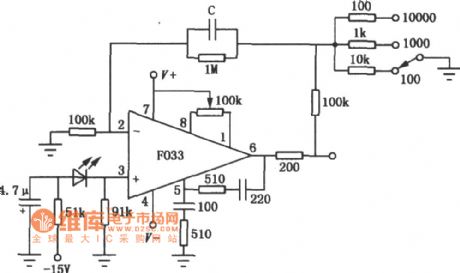
When the incident light illumination changes, it will generate a certain current on optical device. Because the photosensitive signal is very weak, it is better to choose the operational amplifier which has a low input bias current. The sensitive signal amplification circuit composed of the op amp F033 is shown as above. In order to eliminate oscillations, parallel connecting a small capacitor C (pF orders of magnitude) in the feedback circuit. The value of C has a influence on the bandwidth of the amplifier. The DC gain of the circuit is l00, 1000,10000. You can use gain to choose switch and make the corresponding 10kΩ, 1kΩ, 100Ω resistor connect to the ground to achieve. The resistor accuracy of the circuit must be better than ± 1%. The phototube uses FPT102 or FPT100. (View)
View full Circuit Diagram | Comments | Reading(570)
LM324 Single dual power general-purpose quad op amp circuit diagram
Published:2011/5/16 8:32:00 Author:Rebekka | Keyword: Single dual power, general-purpose quad op amp
LM324 is a high-gain op amp contains four units. Its features are: It can both work in single-supply and dual-supply. And it also can work in a wide supply voltage range. And the supply current is small. The input bias current is with temperature compensation. It's not need external frequency compensation components. LM324 can be used for convert amplifier, the DC gain unit and general-purpose op amp application circuits. It can be also used for a variety of logic circuits and other low-pressure system interface circuits. The similar or direct substitution models are: LMl24, CFl24MD, CF224LD, CFl24MJ, CF224LJ, CF324CJ, CF324CP and so on. The LM324 double-threshold voltage comparator circuit is shown as above. (View)
View full Circuit Diagram | Comments | Reading(4803)
CF353 dual power high input impedance dual op amp circuit diagram
Published:2011/6/27 4:41:00 Author:Rebekka | Keyword: Dual power high input, impedance dual op amp
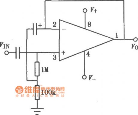
CF353 contains two identical op amps, their input stage is high-speed JFET. It has a high input impedance, low input current and supply current, low noise, offset voltage regulator equipped is a small offset voltage. It has a wide passband and it can be used for high-speed integrators, fast D / A converter sampling a maintain of the circuit. The substitution models are CF353CT, CF353CD, CF353CJ, CF353CP and so on. (View)
View full Circuit Diagram | Comments | Reading(607)
The gain -10 and +11 precision amplifier circuit diagram
Published:2011/6/28 4:26:00 Author:Rebekka | Keyword: precision amplifier
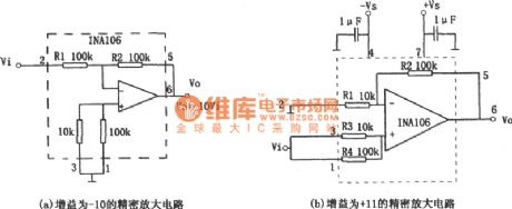
Gain + 11 precision amplifier circuit is shown in figure (b). The amplifier circuit has input impedance high magnification and the voltage is high. The voltage magnification is decided by: Av = type (1 + R2 / R1) = (1 + 100/10) = 1, the maximum gain error of the above two circuits is about 0.01%, The biggest nonlinear error is about 0.001%, the gain drift is about 2 x 10⁻⁶ / ℃. (View)
View full Circuit Diagram | Comments | Reading(605)
Variable gain amplifier circuit diagram
Published:2011/6/30 2:51:00 Author:Rebekka | Keyword: Variable gain amplifier
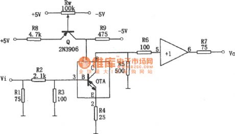

Figure 1 shows the variable gain amplifier (OPA660) circuit chart 1
The OPA660 OTA transconductance gm and static current Io the approximate relationship table.
The figure shows the circuit using transconductance op-amp integrated amplifier amplification OPA660 chip as components. The OPA660 integrated chips internal circuit has two components: The transconductance amplification and caching OTA part. About the internal structure of the integrated chips OPA660, the feet and the main parameters of the relevant material. The figure below is the table of the OPA660 OTA transconductance of gm and static current Io approximate relationship.
(View)
View full Circuit Diagram | Comments | Reading(849)
The high voltage output amplifying circuit composed of high op amp 3583
Published:2011/6/28 4:36:00 Author:Rebekka | Keyword: high voltage output, amplifying circuit
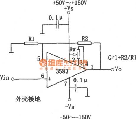
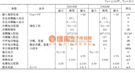
The figure shows the high voltage output amplifier circuit. The high operational amplifier 3583 chip supply voltage range is + 50 ~ + 150 V, the output voltage Vo range is + 40 ~ + 140 V. The voltage magnification is Av = 1 + R2 / R1. The maximum output current is + 75 mA. In 3583 integrated chips internal design overheated shut off the protection circuit, when the output of short circuit can protect integrated chips. It will not be damaged. The positive and negative power are decoupling capacitor. Its value is about 0.1 u F.
(View)
View full Circuit Diagram | Comments | Reading(1238)
10 A power amplifier circuit composed of the OPA541
Published:2011/7/2 1:30:00 Author:Rebekka | Keyword: power amplifier
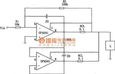
In actual work, in order to drive the motor or incentive the synchronous motor, it often need large current power amplifier circuit. A continuous outputing 10 A current power amplifier is shown in figure. The circuit uses two pieces of high power single piece operational amplifier OPA541 parallel work. The OPA541 monolithic op-amp can output 5 A current (its output current peak can reach up to 10 A), the two pieces of OPA541 parallel available sequential output 10 A current. (View)
View full Circuit Diagram | Comments | Reading(2362)
The resistance electric bridge amplifying circuit composed of the INA102
Published:2011/6/28 4:42:00 Author:Rebekka | Keyword: resistance electric bridge , amplifying circuit
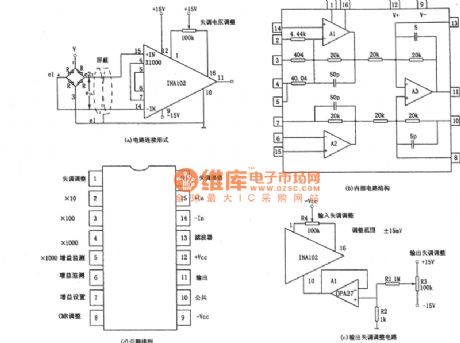
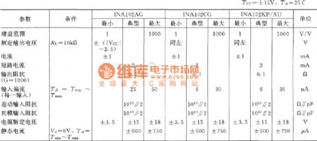
INA102 interior contains three integrated op-amp and resistance components. It has the ability of differential signal amplifier faint. It is often used as the data detection system preamplifier. When the voltage smaller (such as Av amplification times more than 10), the voltage and drift of disorders such as INA102 index can meet the requirements. When the voltage magnification is large (such as Av > 100 large). The bias current imbalance causing disorder voltage error will be bigger. It often uses graph (c) shows circuit to adjust the imbalance INA102 voltage.
(View)
View full Circuit Diagram | Comments | Reading(1098)
The biological electrical signals preamplifier circuit composed of the INA102
Published:2011/6/30 21:35:00 Author:Rebekka | Keyword: biological electrical signals , preamplifier
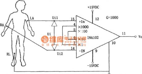
The figure shows the biological signals preamplifier circuit. They need to measure the biological electrical signals of the human body in the medical instrument, such as the electrocardiogram, eeg, etc. Due to the creatures signal is weak, the requirements of the amplifier circuit is very high. This circuit chooses the low power consumption meter with the integrated op-amp INA102. The features of the integrated chips INA102 are: Static current small (maximum is 750 mu A); The internal gain can pass the tube feet and change, the different connecting choice of gain is: l, 10, 100 and 1000 in the photo, pins 4 and 7 are connected with 5, and 6 pins and get the biggest gain 1000. (View)
View full Circuit Diagram | Comments | Reading(1219)
Multilevel parallel connection improved SNR amplifier circuit diagram
Published:2011/6/29 0:59:00 Author:Rebekka | Keyword: multilevel parallel connection, improved SNR amplifier
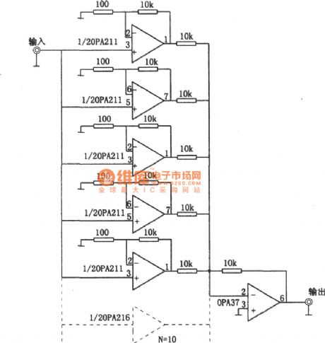
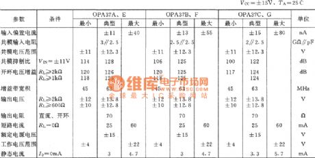
Theop-amp integrated the main parameters of the OPA37:
The input stage amplifier uses multistage parallel to improve the SNR of the amplifier circuit. This is because the input signal voltage is amplified by parallel multistage amplifier circuit and then passes the second amplifier peace. The total output voltage will be increased many times. This multiple is equal to the input stage parallel series. It is shown in figure and gives level l0 input shunt amplifier circuit for the first oder, and the second oder uses reverse phase peace circuit. If the input level is n level, the input signal output voltage will be improved for many times. (View)
View full Circuit Diagram | Comments | Reading(1109)
24dB two-way transmission isolation amplifier circuit composed of the OPA676
Published:2011/6/29 0:16:00 Author:Rebekka | Keyword: 24dB two-way transmission , isolation amplifier
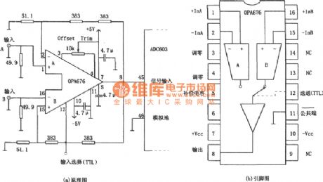
The integrated chip's main parameters of the OPA676:
The figure shows the 24 dB two way transmission buffer amplifier circuit. It is widely used in many aspects. The OPA676 is a typical high-speed operation amplifier circuit, and its special use in the internal containing two ways. And each other is completely independent but its characteristics are completely symmetrical differential input level. The two input levels can be selected by TTL logic level. In other words, the OPA676 has two signal transmission channels, it is respectively marked as A and B channel. The OPA676 chip 12 pins are chosen ends of A, B channel.
(View)
View full Circuit Diagram | Comments | Reading(570)
Microphone Input Signal Amplifier Circuit
Published:2011/7/14 6:28:00 Author:Sue | Keyword: Microphone, Input Signal, Amplifier
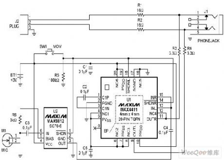
The earphone amplifier(U1,MAX4411) and the microphone amplifier(U2,MAX9812) can use 3v battery as supply power directly. When it is in standard mode, these two appliances are both disconnected, which will consume extra-low battery current. When there is need to talk with others, only the transient switch SW1 should be pushed to start the microphone. Then the microphone's amplifier's bias output will be opened which can amplify the outside audio signal. Then connect the amplified signal to the earphone amplifier and put it into earphone's audio signal through resistor R3,R4. Another advantage of such mix method is that the earphone amplifier's low-impedance(when started) can decay the earphone access's audio current. (View)
View full Circuit Diagram | Comments | Reading(687)
Video Capture Circuit
Published:2011/7/20 7:26:00 Author:Sue | Keyword: Video Capture
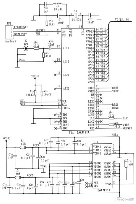
The video decoder this system uses is Philip company's high-performance video A/D converter SAA7111. The device is high-performance video input processor which is widely used in desktop video, multi-media, digital television, photo processing, visual telephone. It uses 3.3V CMOS circuit and highly integrated analog front end and digital video encoder which include two circuits of analog video processing channel, one clock generating circuit, one automatic clamp and gain control circuit, one multi system digital decoder, one brightness/contrast/saturation control circuit, and a color space matrix. (View)
View full Circuit Diagram | Comments | Reading(1748)
| Pages:171/250 At 20161162163164165166167168169170171172173174175176177178179180Under 20 |
Circuit Categories
power supply circuit
Amplifier Circuit
Basic Circuit
LED and Light Circuit
Sensor Circuit
Signal Processing
Electrical Equipment Circuit
Control Circuit
Remote Control Circuit
A/D-D/A Converter Circuit
Audio Circuit
Measuring and Test Circuit
Communication Circuit
Computer-Related Circuit
555 Circuit
Automotive Circuit
Repairing Circuit