
Index 168
20_W_450_MHz_AMPLIFIER
Published:2009/6/18 1:41:00 Author:May
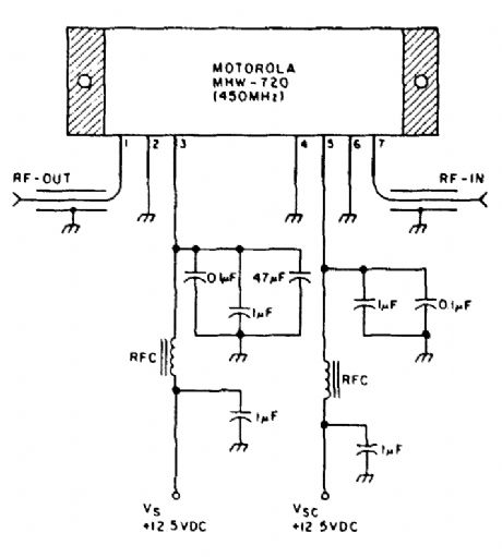
Delivering 20-W output, this amplifier has a gain of 21 dB at 450 MHz. A 12-V supply powers this circuit. (View)
View full Circuit Diagram | Comments | Reading(777)
30_MHz_AMPLIFIER
Published:2009/6/18 1:40:00 Author:May
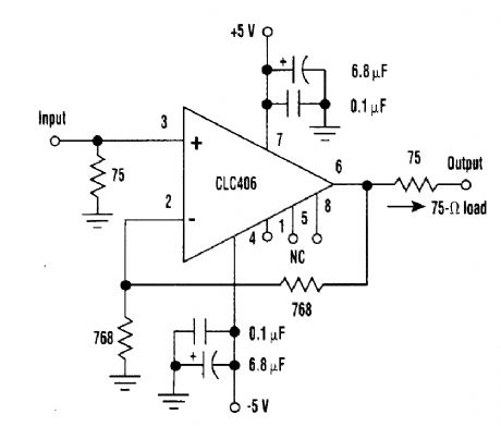
Using a CLC406 op amp, this video amplifier has a voltage gain of +2 and is flat to 30 MHz. The circuit should be useable in video switching and interfacing applications. (View)
View full Circuit Diagram | Comments | Reading(785)
MINIATURE_WIDEBAND_AMPLIFIER
Published:2009/6/17 23:39:00 Author:May
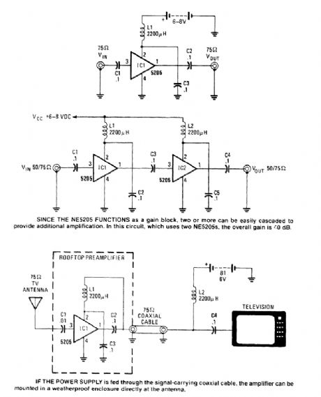
Except for the coupling and decoupling capacitors, IC1 is a complete wideband amplifier that has a fixed gain of 20 dB to 450 MHz. No external compensation is required. (View)
View full Circuit Diagram | Comments | Reading(1208)
70_MHz_RF_POWER_AMPLIFIER
Published:2009/6/17 23:38:00 Author:May
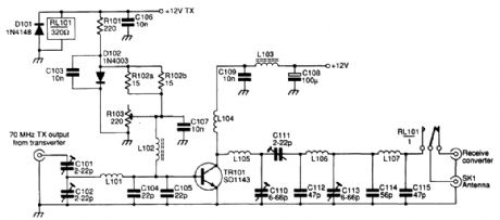
The SD1143 transistor provides a gain of about 14 dB in this circuit. It uses the fact that a 175-MHz device has a much higher gain when used at lower frequencies. The amplifier was originally de-signed to be used with a transverter. The output is 8 to 10 W for a 300- to 500-mW input. (View)
View full Circuit Diagram | Comments | Reading(1392)
BROADCAST_BAND_RF_AMPLIFIER
Published:2009/6/17 23:36:00 Author:May
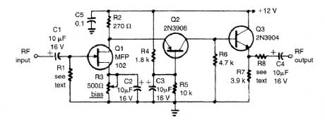
The circuit has a frequency response that ranges from lO0 Hz to 3 MHz; the gain is about 30 dB. Field-effect transistor Q1 is configured in the common-source self-biased mode; optional resistor R1 allows you to set the input impedance to any desired value. Commonly, it will be 50 Ω. The signal is then direct-coupled to Q2, a common-base circuit that isolates the input and output stages and pro-vides the amplifier's exceptional stability. Last, Q3 functions as an emitter-follower, to provide low output impedance (about 50 Ω). If you need higher output impedance, include resistor R8. It will af-fect impedance according to this formula:R8≈ROUT - 50. Otherwise, connect output capacitor C4 directly to the emitter of Q3. (View)
View full Circuit Diagram | Comments | Reading(0)
LOW_NOSIE_GASFET_PREAMP_FOR_435_MHz
Published:2009/6/17 23:21:00 Author:May
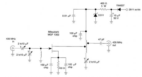
This circuit is a low-noise preamplifier for the 435-MHz amateur satellite frequencies. The cir-cuit uses a Mitsubishi MGF1302. A 28-Vdc source is shown, although by changing the 400-Ω 5-W re-sistor lower voltages can be used. (View)
View full Circuit Diagram | Comments | Reading(1763)
BROADBAND_RF_AMPLIFIER
Published:2009/6/17 23:19:00 Author:May
The use of a FET gives this amplifier a high input impedance. The bandwidth should be ade-quate for LW through HF use (dc-30 MHz), as an active antenna preamplifier. (View)
View full Circuit Diagram | Comments | Reading(3910)
VHF_UHF_PREAMP_USING_MAR_x
Published:2009/6/17 23:17:00 Author:May
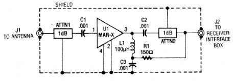
The MAR-x preamp shown will cover up to 1.5 or 2 GHz with the correct MAR-x IC. ATTN1 should be omitted for low noise-figure applications. ATTN1 and ATTN2 provide a means of lirniting possible termination range, for less chance of device instability. (View)
View full Circuit Diagram | Comments | Reading(784)
BUFFER_ISUP2_SUPC_DATA_AND_CLOCK_LINES
Published:2009/6/17 3:15:00 Author:May
The I2C serial bus is a popular two-wire bus for small-area networks. I2C Clock and Data lines have open collector (or drain) outputs for each device on the network. Only a single pull-up resistor is needed. With this architecture, each device can talk on the network, rather than just listen. In some circumstances, it might be desirable to buffer these lines to expand the network, which can sometimes be a tricky task. The obvious approach (Fig. 1) wont work because it latches in either the higher or lower state. A circuit for a noninventory nonlatching buffer is also shown.The circuit is symmetrical about its center so that the input and output can be swapped. Q1 and Q8 are the output open collector drivers. Q2, Q3, Q6, and Q7 provide the nonlatching functions. The capacitors prevent switching glitches by ensuring the inhibit transistors tum off before the output transistors do.Operation can be best explained by example: if the input is high, Q4 turns off, and the voltage across R8 goes to zero. This tums off Q1 and Q8. The output then goes high, which is the circuit's normal resting place. If the input is pulled Iow, Q4 is tumed on.Diode D1 remains reverse-biased, preventing Q3 from tuming off Q4. With Q4 on, current is sup-plied to both Q2 and Q1 to turn them on, but Q2 turns on first to keep Q1 off. This prevents the in-put from latching. Q4 also turns on Q8. D4 is now forward-biased, so Q6 tums on, and thus tums off Q5. With Q5 off, Q7 will not tum on. The output remains low. Even with both the input and the out-put extemally driven low, the circuit will not latch. The circuit, using the values shown in Fig. 2, reached a clock rate of 80 kHz with a VOH of 5.0 V and a VOL of 0.5 V. (View)
View full Circuit Diagram | Comments | Reading(681)
LOW_OFFSET_SIMPLE_VIDEO_BUFFER
Published:2009/6/17 2:13:00 Author:May
This circuit has proved to be an effective video buffer and will easily drive a 75-Ω load to 1.5-V p-p output. BW is better than 20 MHz and there is less than 0.05-V dc offset, which is the difference inVBE of Q1 and Q2. The supply lines should be well bypassed, ± 5V or more. (View)
View full Circuit Diagram | Comments | Reading(1396)
3_V_RAIL_TO_RAIL_SINGLE_SUPPLY_BUFFER
Published:2009/6/17 2:11:00 Author:May
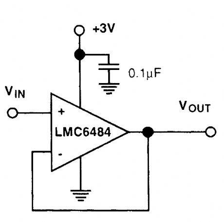
The LMC6484 provides a 3-V p-p rail-to-rail buffer with a +3-V supply commonly used for logic systems. (View)
View full Circuit Diagram | Comments | Reading(697)
SIMPLE_VIDEO_BUFFER
Published:2009/6/17 2:10:00 Author:May

This simple emitter follower can be used as a video buffer. (View)
View full Circuit Diagram | Comments | Reading(4157)
MOSFET_BUFFER_AMPLIFIER
Published:2009/6/17 2:09:00 Author:May
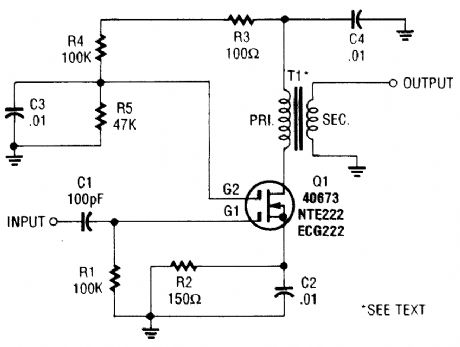
A MOSFET is used as a wideband buffer amplifier. T1 is wound on a toroid of approximately 1/2 diameter, with material suitable for frequency (usually 1- to 20-MHz range). The turns ratio should be about 4:1 depending on load imped-ance. Typically, at 4 MHz, there are 18 turns on the primary, 4 turns on the secondary, and the stage gain is about 14-dB voltage (ZL = 50 Ω). (View)
View full Circuit Diagram | Comments | Reading(1093)
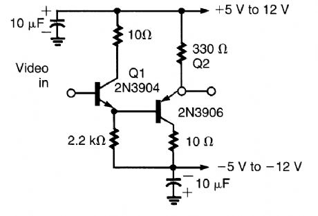
VFO_BUFFER_AMPLIFIER
Published:2009/6/17 2:06:00 Author:May
A two-transistor feedback pair provides broadband operation. The gain is approximately R4/R1. (View)
View full Circuit Diagram | Comments | Reading(1304)
HIGH_CURRENT_BUFFER
Published:2009/6/17 2:03:00 Author:May
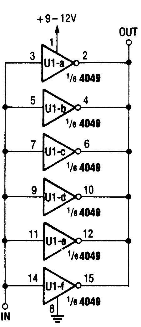
By parallel connecttng all six gates of this 4049 hex inverting buffer,you can obtain a much higher output current than would othewise be available. (View)
View full Circuit Diagram | Comments | Reading(996)
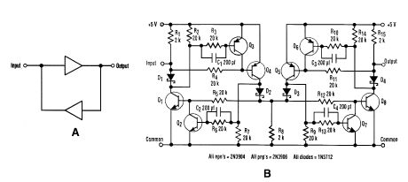
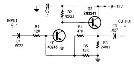
BUFFER_AMPLIFIERS
Published:2009/6/17 2:00:00 Author:May
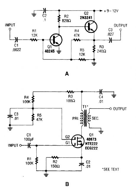
These two buffer/amplifiers that have been successfully used with VFOs: one (shown in A) is based on a pair of bipolar npn transistors, and the other (shown in B) is built around a dual-gate MOSFET. (View)
View full Circuit Diagram | Comments | Reading(880)
LM6218_HIGH_SPEED_INSTRUMENTATION_AMPLIFIER
Published:2009/6/16 22:53:00 Author:May
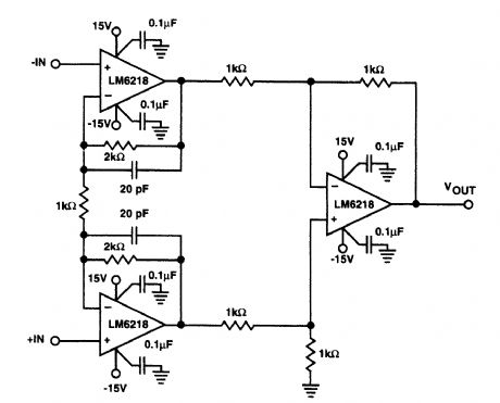
This amplifier features 400-μsec settling time (to 0.01%), 140-V/psec slow rate, and 17-MHz gain-bandwidth product. The supply voltage can be ±5 to ±20V. (View)
View full Circuit Diagram | Comments | Reading(682)
LMC6062_INSTRUMENTATION_AMPLIFIER
Published:2009/6/16 22:41:00 Author:May
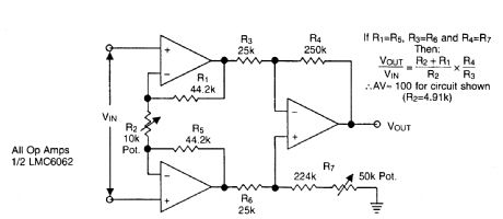
Useful for +5-V single-supply applications, this op amp circuit features low drain (around 1 mA), high input resistance (1014Ω), and low bias current (≈10-14A). (View)
View full Circuit Diagram | Comments | Reading(784)
NONINVERTING_ac_AMPLIFIER
Published:2009/6/15 2:32:00 Author:May
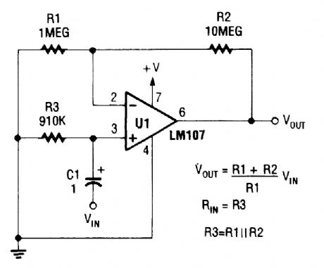
A general-purpose noninverting ac amplifier for audio of other low-frequency applications is shown. Design equations are in the figure. Almost any general-purpose op amp can be used for U1. (View)
View full Circuit Diagram | Comments | Reading(670)
AUDIO_DISTRIBUTION_AMPLIFIER
Published:2009/6/15 23:13:00 Author:May
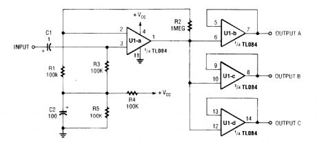
Three low-Z audio outputs are available from this circuit, using a quad TL084 FET amplifier. The input is high impedance. VCC can be 6 to 12 V for typical applications. (View)
View full Circuit Diagram | Comments | Reading(6610)
| Pages:168/250 At 20161162163164165166167168169170171172173174175176177178179180Under 20 |
Circuit Categories
power supply circuit
Amplifier Circuit
Basic Circuit
LED and Light Circuit
Sensor Circuit
Signal Processing
Electrical Equipment Circuit
Control Circuit
Remote Control Circuit
A/D-D/A Converter Circuit
Audio Circuit
Measuring and Test Circuit
Communication Circuit
Computer-Related Circuit
555 Circuit
Automotive Circuit
Repairing Circuit