
Index 162
SIMPLE_BIDIRECTIONAL_BUFFER_DESIGN
Published:2009/6/22 22:47:00 Author:Jessie
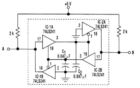
This circuit shown in the figure uses two 74LS241s. When both input/output lines are high, IC-1A and IC-2B turn on, and C1 and CZ are charged to high voltage. Meanwhile, IC-1B and IC-2A are off to prevent a logic 1 latch. (View)
View full Circuit Diagram | Comments | Reading(1294)
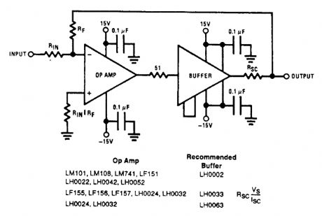
VOLTAGE_FOLLOWER
Published:2009/6/22 22:46:00 Author:Jessie
View full Circuit Diagram | Comments | Reading(127)
ANALOG_NONINVERTING_SWITCHED_BUFFER
Published:2009/6/22 22:44:00 Author:May
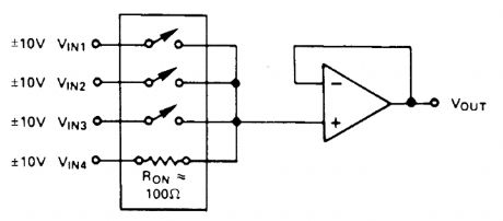
Here is noninverting solution. (View)
View full Circuit Diagram | Comments | Reading(528)
SINGLE_SUPPLY_ac_BUFFER_AMPLIFIER
Published:2009/6/22 22:44:00 Author:May
This buffer Right be used with a single sup-ply without special considerations. The input is dc biased to mid-operating point and is ac cou-pled. Its input impedance is approximately 500 kΩ at low frequencies. Note that for dc loads ref-erenced to ground, this quiescent current is in-creased by the load current set at the input dc bias voltage. (View)
View full Circuit Diagram | Comments | Reading(1168)
SINGLE_SUPPLY_PHOTODIODE_AMPLIFIER
Published:2009/6/22 22:44:00 Author:May
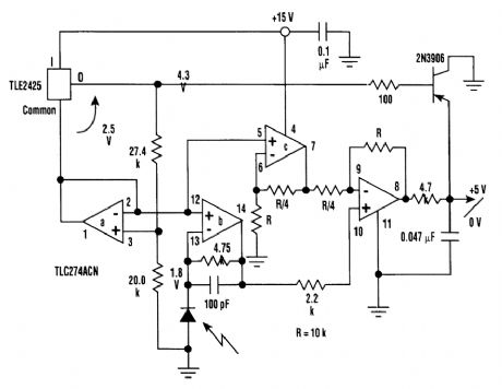
This circuit provides a reverse-bias operating point and output voltage offset and uses a single-polarity power supply. The floating reference voltage from TLE2425 serves to bias the diode in a reverse-polarity mode. It also provides a clamping level at the output. Consequently, linear response to illumination is maintained for a 5-V range from dark current to full sunlight conditions. (View)
View full Circuit Diagram | Comments | Reading(1452)
ADC_BUFFER
Published:2009/6/22 22:42:00 Author:May

Useful for driving high-speed, 10-bit ADCs, this circuit was developed to drive an 18-MSPS 10-bit ADS. It works from ±5-V supplies. (View)
View full Circuit Diagram | Comments | Reading(758)
WIDEBAND_GENERAL_PURPOSE_BUFFER
Published:2009/6/22 22:41:00 Author:May
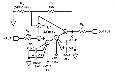
This circuit has unity gain and response up to 70 MHz. UI is an Analog Devices AD817. (View)
View full Circuit Diagram | Comments | Reading(747)
HI_Z_MICROPHONE_BUFFER_AMPLIFIER
Published:2009/6/22 22:39:00 Author:May
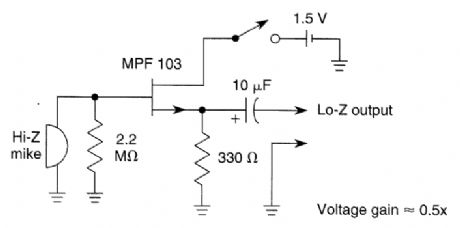
A low impedance output from a high-Z microphone can be obtained with this circuit. No voltage gain is obtained, but a power gain is obtained because the output impedance is much lower (300 Ω), with -6-dB voltage gain. (View)
View full Circuit Diagram | Comments | Reading(936)
UNITY_GAIN_ADC_BUFFER
Published:2009/6/22 22:39:00 Author:May
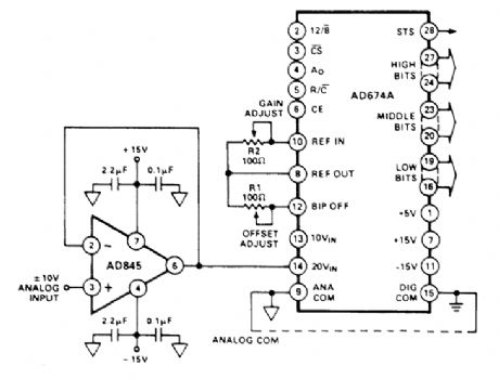
This buffer is suitable for ADCs of 12 bits bandwidth of 5μs or greater.The wide bandwidth of the AD845 ensures a low output impedance at higher frequencies in the voltage follower (buffer) configuration. (View)
View full Circuit Diagram | Comments | Reading(743)
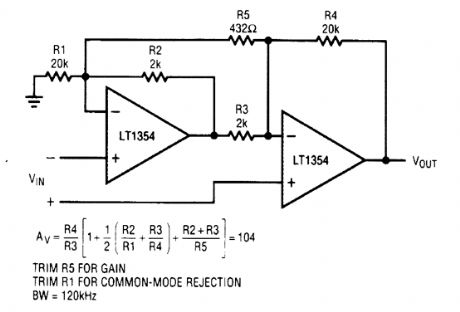
BRIDGE_AMPLIFIER_WITH_LOW_NOISE_COMPENSATION
Published:2009/6/22 22:35:00 Author:May
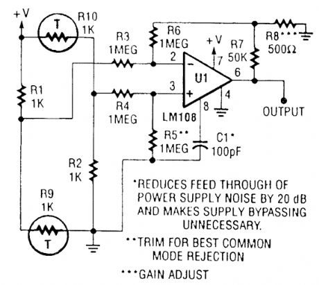
View full Circuit Diagram | Comments | Reading(1064)
SINGLE_SUPPLY_BRIDGE_AMPLIFIER
Published:2009/6/22 22:33:00 Author:May
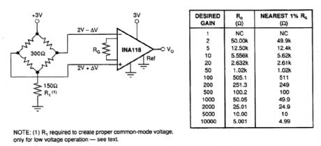
The INA118 can be used on single-power supplies of +2.7 to +36V. The figure shown is a basic single-supply circuit. The output Ref terminal is connected to ground. Zero differential input voltage will dentand an output voltage of 0V (ground). Actual output voltage swing is limited to approxi-mately 35 mV above ground, when the load is referred to ground as shown. The typical performance curve “Output Voltage”, Output Current shows how the output voltage swing varies with output current.
With single-supply operation, +VIN and -VIN must both be 1.1V above ground for linear operation. You cannot, for instance, connect the inverting input to ground and measure a voltage connected to the noninverting input.To illustrate the issues affecting low-voltage operation, consider the circuit in the figure. It shows the INA118, operating from a single 3-V supply. A resistor in series with the low side of the bridge en-sures that the bridge output voltage is within the common-rqode range of the amplifier's inputs. (View)
View full Circuit Diagram | Comments | Reading(1758)
OP_AMP_DIODE_LASER_DRIVER
Published:2009/6/22 22:31:00 Author:May
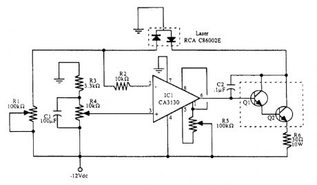
This circuit is one way to automatically adjust drive current using a discrete op amp. Use the transistors specified or replace them with a suitable Darlington power transistor (such as TIP 120).IC1RCA CA 313 operational amplifierR1,R5 100-kΩ potentiometerR2 10-kΩ resistorR3 3.3-kΩ potentiometerR4 10-kΩ potentiometerR6 30-Ω, 10-W resistorC1100-μF electrolytic capacitorC2 0.1-μF disc capacitorQ1 2N2101 transistorQ2 2N3585 transistorLaser RCA C86002 (or equivalent laser diode) (View)
View full Circuit Diagram | Comments | Reading(2396)
Tube Power Amplifier circuit diagram(with power source)
Published:2011/7/20 20:09:00 Author:Ecco | Keyword: Tube Power Amplifier , power source
If the power amplifier coupled with good speakers and good environment, and DVD audio playback, it likes the power amplifier with the price in a few thousand dollars. The following is the power circuit diagram:
(View)
View full Circuit Diagram | Comments | Reading(715)
VEHICLE_AUDIO_AMPLIFIER_INVERTER
Published:2009/6/19 4:53:00 Author:May
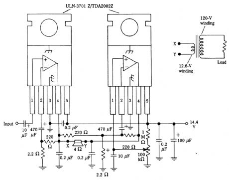
An audio amplifier can drive a step-up transformer to obtain 120 Vac. (View)
View full Circuit Diagram | Comments | Reading(1019)
ELECTRONICALLY_CONTROLLED_VARIABLE_GAIN_VIDEO_LOOP_THROUGH_AMPLIFIER__
Published:2009/6/19 4:51:00 Author:May
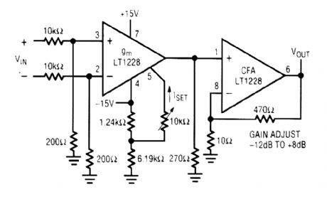
An LT1228 transconductance amplifier iS used in this application The gain is adjustable from-12to+8dB. (View)
View full Circuit Diagram | Comments | Reading(627)
DIFFERENTIAL_VIDEO_LOOP_THROUGH_AMPLIFIER
Published:2009/6/19 4:47:00 Author:May
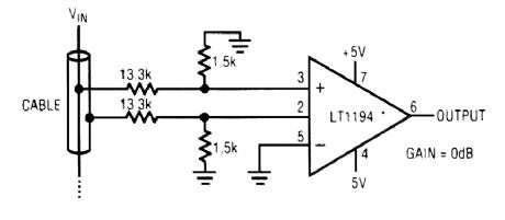
An LT1194 is used as a differential amplifier for video applications, where low cable loading is needed. (View)
View full Circuit Diagram | Comments | Reading(744)
SIMPLE_VIDEO_AMPLIFIER
Published:2009/6/19 4:38:00 Author:May
Useful for interfacing B/W TV sets with a camera or computer, this amplifier has a bandwidth of ≥10 MHz and a gain of 3X. (View)
View full Circuit Diagram | Comments | Reading(1447)
2INSTRUMENTATION_AMPLIFIER
Published:2009/6/19 4:38:00 Author:May
View full Circuit Diagram | Comments | Reading(841)
ULTRA_LOW_NOISE_SINGLE_SUPPLY_INSTRUMENTATION_AMPLIFIER
Published:2009/6/19 4:35:00 Author:May
View full Circuit Diagram | Comments | Reading(731)
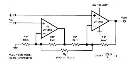
LOW_POWER_INSTRUMENTATION_AMPLIFIER
Published:2009/6/19 4:34:00 Author:May

This amplifier requires less than 20 mA from a ±15-V supply. (View)
View full Circuit Diagram | Comments | Reading(808)
| Pages:162/250 At 20161162163164165166167168169170171172173174175176177178179180Under 20 |
Circuit Categories
power supply circuit
Amplifier Circuit
Basic Circuit
LED and Light Circuit
Sensor Circuit
Signal Processing
Electrical Equipment Circuit
Control Circuit
Remote Control Circuit
A/D-D/A Converter Circuit
Audio Circuit
Measuring and Test Circuit
Communication Circuit
Computer-Related Circuit
555 Circuit
Automotive Circuit
Repairing Circuit