
Index 170
TEST_BENCH_AMPLIFIER
Published:2009/6/15 4:08:00 Author:May
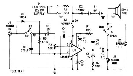
This amplifier might be useful in senricing or bench testing as a signal tracer or as a building block in various systems. (View)
View full Circuit Diagram | Comments | Reading(2407)
CURRENT_FEEDBACK_AMP_DELIVERS_100mA__100MHz
Published:2009/6/15 4:05:00 Author:May

Using a NS LM6181, this IC is useful in cable drivers. The supply voltage is ±5V to ±15V. (View)
View full Circuit Diagram | Comments | Reading(603)
V__I_PROTECTED_INTRINSICALLY_SAFE_OP_AMP
Published:2009/6/15 4:05:00 Author:May
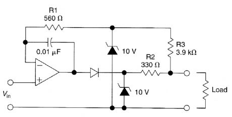
The circuit is designed to drive an external load. A fault condition in the external load circuit could feed excessive current or voltage back into the line drive circuit. If excessive voltage appears from the load, the two zener diodes will clamp that voltage to a safe level, which in this case is 10V.The current in the zener diodes, op amp, and the remainder of the circuitry is limited to a safe level by resistors R1, R2, and R3. D1 protects the op-amp output stage from 10V appearing across the clamp diodes under a fault condition.The advantage of this circuit is that, although it's designed as unity gain buffer, the same tech-niques can be applied to inverting, noninverting, or differential gain stages. (View)
View full Circuit Diagram | Comments | Reading(826)
DISCRETE_CURRENT_BOOSTER_AMPLIFIER
Published:2009/6/15 3:48:00 Author:May
Suitable as a line driver, this circuit is useable in many similar audio applications. (View)
View full Circuit Diagram | Comments | Reading(754)
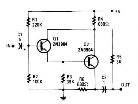
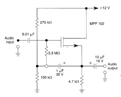
500_MΩ_INPUT_IMPEDANCE_WITH_JFET_AMP
Published:2009/6/15 3:47:00 Author:May
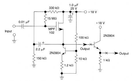
A current source using a 2N3904 transistor plus bootstrapping, achieves an input impedance of 500MΩ. A second 2N3904 transistor can be added at X to lower the output impedance. (View)
View full Circuit Diagram | Comments | Reading(1151)
NONINVERTED_UNITY_GAIN_AMPLIFIER
Published:2009/6/15 3:33:00 Author:May
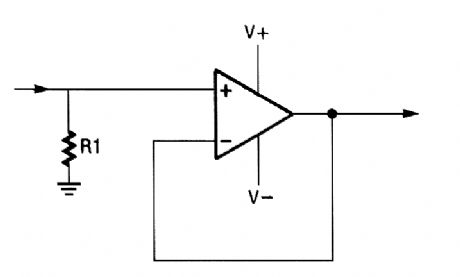
An op amp can be used as a unity gain am-plifier by connecting its output to its inverting input as shown. R1 should be low enough so the bias current of the op amp does not cause an ap-preciable offset. (View)
View full Circuit Diagram | Comments | Reading(660)
PUSH_PULL_DARLINGTON_AMPLIFIER
Published:2009/6/15 3:32:00 Author:May
This circuit has a high-Z input and push-pull output via the output taken across R4 and R6. (View)
View full Circuit Diagram | Comments | Reading(1579)
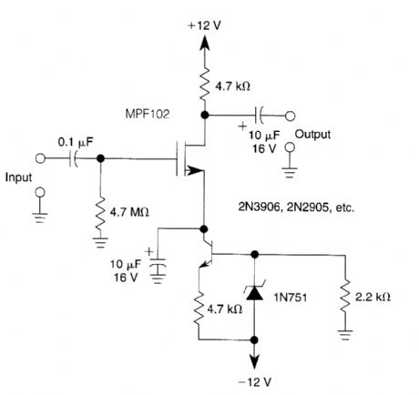
FET_AMPLIFIER_WITH_OFFSET_GATE_BIAS
Published:2009/6/15 3:31:00 Author:May
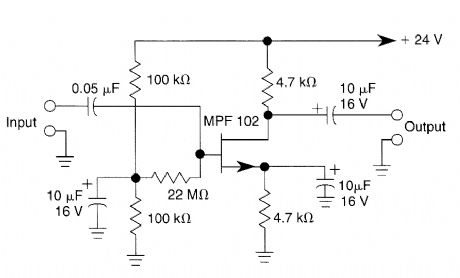
In this amplifier circuit, the gate of the MPF102 is biased with an external voltage. This circuit achieves tighter control of the operating point and biasing conditions. (View)
View full Circuit Diagram | Comments | Reading(1003)
ELECTRET_MIKE_PREAMP
Published:2009/6/15 3:18:00 Author:May
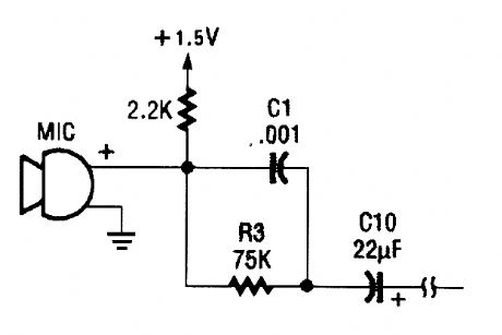
This circuit is suitable for using an electret microphone for many applications. A 1.5-V bat-tery is used. C1 and R3 provide treble boost/bass cut; they can be eliminated, if desired. (View)
View full Circuit Diagram | Comments | Reading(2349)
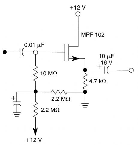
JFET_AMP_WITH_CURRENT_SOURCE_BIASING
Published:2009/6/15 3:18:00 Author:May
A current source (MPF102) in the source lead of bipolar transistor 2N3906 permits accurate control of drain current. (View)
View full Circuit Diagram | Comments | Reading(1590)
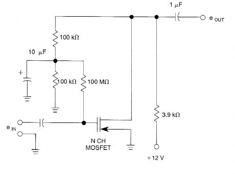
UNITY_GAIN_NONINVERTING_AMPLIFIER
Published:2009/6/15 3:17:00 Author:May
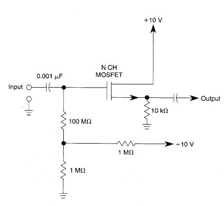
Biasing methods for an N-channel MOSFET to form a unity-gain noninverting amplifier or source-follower. (View)
View full Circuit Diagram | Comments | Reading(666)
JFET_SOUTCE_FOLLOWER
Published:2009/6/15 3:03:00 Author:May
The circuit uses positive gate bias to improve the operating point for better dynamic range. (View)
View full Circuit Diagram | Comments | Reading(848)
30_MΩ_JFET_SOURCE_FOLLOWER
Published:2009/6/15 3:01:00 Author:May
This JFET source-follower uses an MPF102 with offset biasing. It has an input impedance of >30MΩ (View)
View full Circuit Diagram | Comments | Reading(1199)
BOOTSTRAPPED_SOURCE_FOLLOWER
Published:2009/6/15 2:58:00 Author:May
This bootstrapped Source follower uses an N-channel MOSFET.It has a high input impedance. (View)
View full Circuit Diagram | Comments | Reading(907)
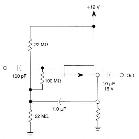
MOSFET_HIGH_IMPEDANCE_BIASING_METHOD
Published:2009/6/15 2:54:00 Author:May
High-impedance biasing method for an N-channel MOSFET to form a linear-inverting amplifier. (View)
View full Circuit Diagram | Comments | Reading(635)
NONLINEAR_OPERATIONAL_AMPLIFIER_WITH_TEMPERATURE_COMPENSATED_BREAKPOINT
Published:2009/6/15 2:53:00 Author:May
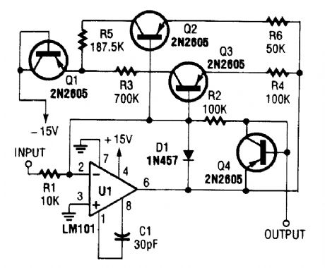
View full Circuit Diagram | Comments | Reading(702)
INVERTING_SUMMING_AMPLIFIER
Published:2009/6/15 2:38:00 Author:May
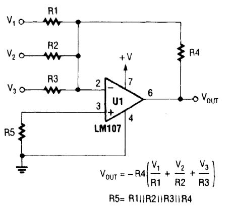
The out put of U1 is the sum of V1, V2, and V3, multiplied by R1/R4, R1/R4, and respectively. R1, R2, R3 are selected as required for individual gains. R4 affects gain of all these inputs. (View)
View full Circuit Diagram | Comments | Reading(1403)
FAST_INVERTING_AMPLIFIER_WITH_HIGH_INPUT_IMPEDANCE
Published:2009/6/15 2:27:00 Author:May
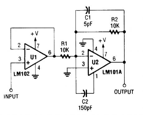
U1 is used as a voltage follower to feed in-verter U2. Because UI is in the voltage-follower configuration, it exhibits a high input impedance. (View)
View full Circuit Diagram | Comments | Reading(1262)
DIFFERENCE_AMPLIFIER
Published:2009/6/15 2:25:00 Author:May
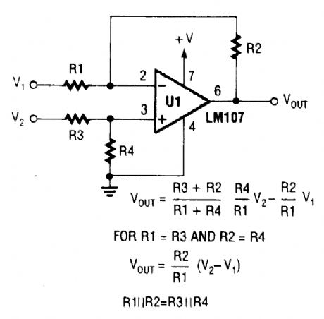
By using two inputs as shown, a difference amplifier yielding the differential between U1 and U2, times a gain factor results. (View)
View full Circuit Diagram | Comments | Reading(1563)
PARALLEL_LOOP_ALARM
Published:2009/6/14 21:39:00 Author:jailer
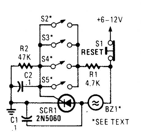
Four paraJlel switches are used to monitor four positions. When a closure occurs on any switch, SCR1 triggers, which sounds the alarm.The alarm should be of the noninterrupting type. (View)
View full Circuit Diagram | Comments | Reading(735)
| Pages:170/250 At 20161162163164165166167168169170171172173174175176177178179180Under 20 |
Circuit Categories
power supply circuit
Amplifier Circuit
Basic Circuit
LED and Light Circuit
Sensor Circuit
Signal Processing
Electrical Equipment Circuit
Control Circuit
Remote Control Circuit
A/D-D/A Converter Circuit
Audio Circuit
Measuring and Test Circuit
Communication Circuit
Computer-Related Circuit
555 Circuit
Automotive Circuit
Repairing Circuit