
Index 164
100_W_VARIABLE_RESISTOR_SIMULATOR
Published:2009/6/19 4:09:00 Author:May
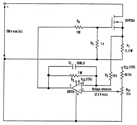
Variable resistive loads with precise load steps often are required in automatic testers used to test and calibrate power supplies. The action of a high-power(100 W)variable resistor can be simu-lated with the circuit shown.The voltage drop across R1, which is proportional to the FET current, is compared against a vari-able input voltage reference using a high-gain op amp. Error voltage developed by the amplifier drives the gate, controlling the transconductance of the FET.Power dissipation is limited by the safe-operating-area curve of the selected FET. The FET should be mounted onto a properly sized heatsink or a heatsink-fan combination to maintain its case temperature within safe limits. The circuit is designed to dissipate a ntaximum power of 100Wif the FET-case temperature is maintained below 50℃. The potentiometer (RV1) can be replaced by a dig-ital-to-analog converter so that it can adapt to the computer control for use in automatic testers. (View)
View full Circuit Diagram | Comments | Reading(1419)
The compensation circuit of op amp output capacitor
Published:2011/6/27 21:52:00 Author:Rebekka | Keyword: Op amp output capacitor, Compensation circuit
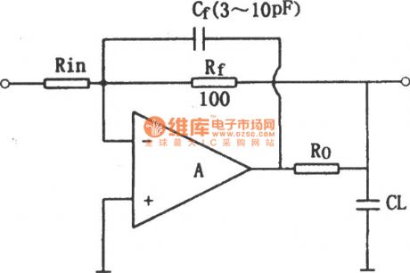
Put a resistance Ro at the output terminal of the series. The load capacitance CL and amplifying circuit is separated, it is shown in figure, connect the feedback resistance Rf in the back of the Ro. This can compensate the dc attenuation. The feedback capacitor Cf will reduce the high frequency closed-loop voltage magnification. The method of selecting Cf is: Make amplifier circuit of the unit gain the RongKang Xcf frequency fT 10, Rf/Xf = l / (2) fTCf PI. Usually, Ro = 50 ~ 200 Ω, Cf is 3 ~ 10 pF. It is shown in figure, the op-amp output capacitance of the compensation circuit diagram.
(View)
View full Circuit Diagram | Comments | Reading(1468)
Variable gain differential amplifier circuit composed of the μA709
Published:2011/6/27 5:14:00 Author:Rebekka | Keyword: Variable gain, differential amplifier
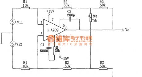
The figure shows variable gain differential amplifier circuit composed of the μA709. The biggest advantage of this circuit is to maintain common-mode rejection and keep the ratio KCMR in the same premise. The differential gain can be achieved continuously adjustable. The biggest advantage of this circuit is to maintain common-mode rejection ratio KCMR the same premise, the differential gain can be achieved continuously adjustable. The circuit of the basic relationship is: Vo =- (2R2/R1) · (1 + R2/R3) · (Vi1-Vi2) Av = Vo / (Vi1 a Vi2) =- (2R2/R1) · (1 + R2 / R3) When R1 = 10kΩ, R2 = 50kΩ, R3 = 5kΩ when, Av =- 110. μA709 integrated chip electrical parameters (VD = ± 15V, TA = 25 ℃). (View)
View full Circuit Diagram | Comments | Reading(1787)
RF2152 dual-mode high-power linear amplifier pin diagram
Published:2011/5/6 1:00:00 Author:May | Keyword: dual-mode, high-power, linear amplifier
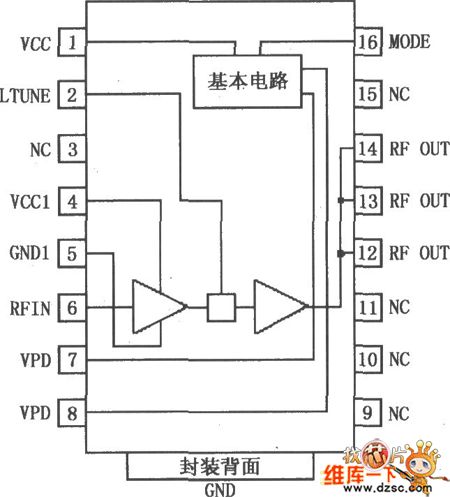
RF2152 is a high-power, high efficiency linear amplifier IC. It is used in 3V handheld systems, such as 3V CDMA/AMPS mobile cellular systems, JD-MA/TACS mobile phone and TDMA/AMPS mobile phone. RF2152 is used advanced GaAs heterojunction bipolar transistor (HBT) to treat. It is intended for dual-mode CDMA/AMPS handheld digital cellular systems devices' final linear RF enlarge, band spread system and other application with 800~950MHz working frequency. The device itself includes 50Ω input and output, so is very easy to get best power, efficiency and linear performance. RF2152 uses PSSOP-16 package, its pin array is shown in the diagram. (View)
View full Circuit Diagram | Comments | Reading(735)
Charge amplifier circuit composed of the OPA128
Published:2011/6/28 3:30:00 Author:Rebekka | Keyword: Charge amplifier
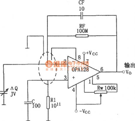
The so-called charge amplifier is amplifier circuit used to amplify the signal from the piezoelectric devices charge. The intrinsic impedance of the amplifier circuit sources is high, while the signal is very weak. The formation of the current source is only pA level. The charge amplifier need to have high input resistance and low offset current. Or when the amplifier's bias current is similar to the signal current signals, the signals might be engulfed by the current. The normal amplification will not be achieved. (View)
View full Circuit Diagram | Comments | Reading(2620)
TWO_AMPLIFIER_FLIP_FLOP
Published:2009/6/19 2:54:00 Author:May

View full Circuit Diagram | Comments | Reading(772)
SIMPLE_TEST_AUDIO_AMPLIFIER
Published:2009/6/19 2:53:00 Author:May
This circuit has a gain of about 20. A suitable power supply voltage is 5 to 12 V, depending on the desired audio output power level. (View)
View full Circuit Diagram | Comments | Reading(757)
ONE_OP_AMP_BANDPASS_FILTER
Published:2009/6/19 2:34:00 Author:May

View full Circuit Diagram | Comments | Reading(1)
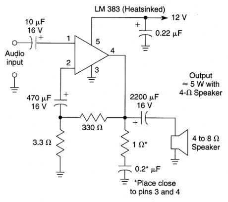
HIGH_POWER_12_V_IC_AUTO_AMPLIFIER
Published:2009/6/19 2:29:00 Author:May
View full Circuit Diagram | Comments | Reading(811)
HIGH_POWER_AUDIO_AMP_FOR_AUTOMOTIVE_INSTALLATION
Published:2009/6/19 2:29:00 Author:May
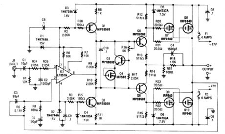
Two of these audio amplifiers can be used to make a stereo amplifier 200W per channel. IRF640 and IRF9640 power MOSFETs are used to drive the output load, which might be 4 or 8Ω. Response is 12 Hz to 45 kHz (-3 dB), THD <0.1%. Power is supplied by a switching-type power supply, which is external to the amplifier (±47V). About 600 W total power (peak) is needed. (View)
View full Circuit Diagram | Comments | Reading(8600)
DC servo isolation amplifier circuit diagram
Published:2011/6/26 21:12:00 Author:Rebekka | Keyword: DC servo, isolation amplifier
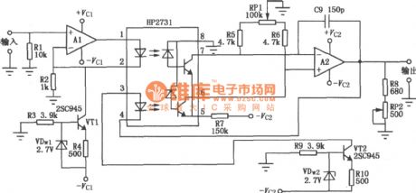
The picture shows the DC isolation servo amplifier circuit. When the analog signals are mixed with mode voltage noise, you can use this circuit to make the sensor input signals impend. In order to transmit the DC signal, the circuit uses servo means to form a feedback circuit to improve the stability of the circuit. A1 uses constant current drive optocoupler HP2731 in the light-emitting diode, the input signal bias current is 4mA. The optocoupler in the circuit uses double-type circuit HP2731. It has tracking performance. (View)
View full Circuit Diagram | Comments | Reading(2231)
90_V_10_A_HIGH_POWER_AMPLIFIER
Published:2009/6/19 2:01:00 Author:May
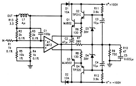
This amplifier can drive ±90 V at 10A, more than twice the output swing of the LM12. The IC provides current and power limiting for the discrete transistors. (View)
View full Circuit Diagram | Comments | Reading(2110)
BRIDGE_CONNECTION_OF_TWO_POWER_op_AMPS
Published:2009/6/19 1:58:00 Author:May
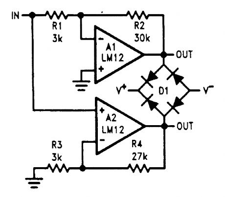
These bridge connections provide differential outputs that approach twice the total supply voltage. Diode bridge clarnps output to the supplies. (View)
View full Circuit Diagram | Comments | Reading(831)
GENERAL_PURPOSE_AF_AMPLIFIER
Published:2009/6/19 1:58:00 Author:May
Schematic of the general-purpose AF amplifier.All resistors are 1/4-W,5%-tolerance carbon-com-position or metal-film units,Equivalent parts can be substituted,General purpose IC replacementsare shown in parentheses (View)
View full Circuit Diagram | Comments | Reading(669)
STEREO_PHONO_AMPLIFIER_WITH_BASS_TONE_CONTROL
Published:2009/6/19 1:57:00 Author:May
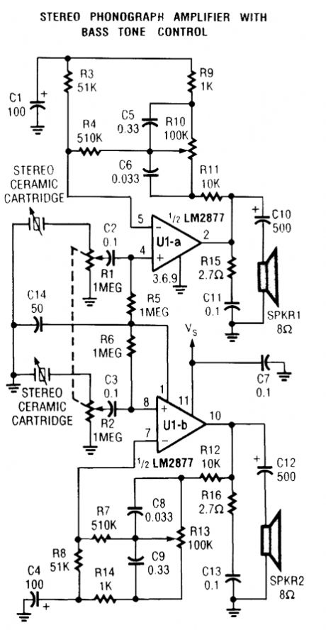
View full Circuit Diagram | Comments | Reading(716)
STEREO_PREAMPLIFIER
Published:2009/6/19 1:55:00 Author:May
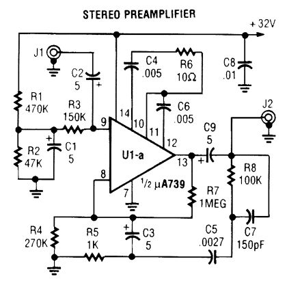
A building block for audio work, the circuit can be used as a general-purpose preamp. Use two circuits for stereo applications. (View)
View full Circuit Diagram | Comments | Reading(923)
BASIC_COMPLEMENTARY_POWER_AMPLIFIER_CIRCUIT
Published:2009/6/19 1:54:00 Author:May
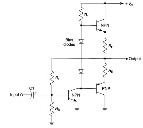
View full Circuit Diagram | Comments | Reading(682)
80_WATT_IC_AUDIO_AMPLIFIER
Published:2009/6/19 1:54:00 Author:May
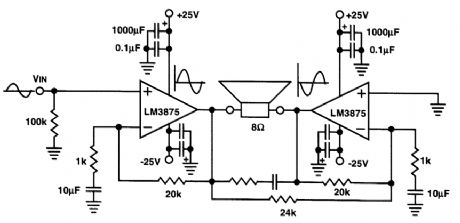
This audio power amp will deliver 80W of audio into an 8-Ω load The LM3875 IC devices shouldbe suitably heatsinked。Note that the amplifier IS a bridged circuit,with both speaker leads“hot.” (View)
View full Circuit Diagram | Comments | Reading(2034)
MINI_STEREO_AMPLIFIER
Published:2009/6/19 1:52:00 Author:May
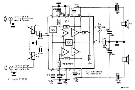
Using a Thomson TEA2025, this stereo amplifier provides 1 W per channel into 4 Ω with a 9-V supply. Input sensitivity is 25 mV p-p for full output. Note that pins 4, 5, 12, and 13 of IC1 should be effectively grounded to a ground plane and heatsinked. (View)
View full Circuit Diagram | Comments | Reading(1187)
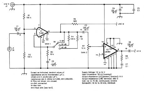
PHONO_AMP
Published:2009/6/19 1:51:00 Author:May
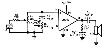
The figure shows the LM380 with a voltage-divider volume control and high-frequency roll-off tone control. (View)
View full Circuit Diagram | Comments | Reading(831)
| Pages:164/250 At 20161162163164165166167168169170171172173174175176177178179180Under 20 |
Circuit Categories
power supply circuit
Amplifier Circuit
Basic Circuit
LED and Light Circuit
Sensor Circuit
Signal Processing
Electrical Equipment Circuit
Control Circuit
Remote Control Circuit
A/D-D/A Converter Circuit
Audio Circuit
Measuring and Test Circuit
Communication Circuit
Computer-Related Circuit
555 Circuit
Automotive Circuit
Repairing Circuit