
Index 144
Norton_low_frequency_mixer
Published:2009/7/25 1:26:00 Author:Jessie
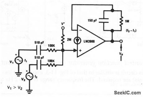
This circuit shows a Norton used as a low-frequency mixer where two input frequencies produce a sum and difference frequency (in addition to other high-frequency components). The circuit has a gain of 10 and a low-pass single-pole filter (1 MΩ and 150 pF) with a comer frequency of 1 kHz. Relatively high frequencies can be applied at the inputs as long as the desired difference frequency is within the bandwidth capabilities of the amplifier and the RC low-pass filter. The difference frequency is filtered from the composite resulting waveform and is made available at the output. (View)
View full Circuit Diagram | Comments | Reading(2356)
4_BIT_BCD_COMPARATOR
Published:2009/6/29 1:47:00 Author:May
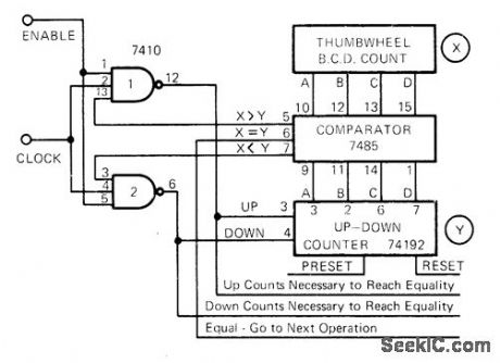
Provides less than, equal to, or greater than comparison between setting of BCD thumbwheel switch at X and BCD input digit at Y (Y is count preset into 74192 up/down counter). If equality does not exist, circuit will count up ordown until it reaches equality, and thereby calculate difference between BCD values. Separate register can be used to store up or down counts required to reach equality.—R. A. Scher, Digital Comparator is Self-Adjusting, EDNMagazine, Sept. 1, 1972, p 51. (View)
View full Circuit Diagram | Comments | Reading(2437)
Triangle_wave_to_sine_wave_converter
Published:2009/7/25 1:16:00 Author:Jessie
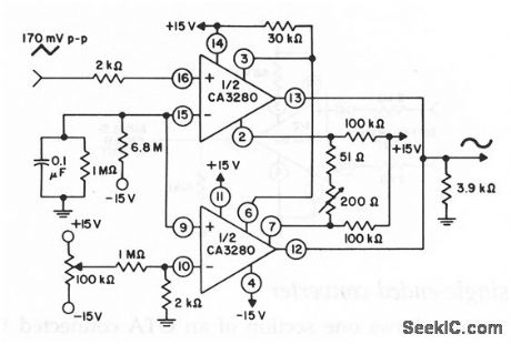
This circuit shows a triangle-wave to sine-wave converter using two sections of an OTA. Two 100-kΩ resistors are connected between the differential-amplifier emitters and U+ to reduce the current flow through the differential amplifier. This allows the amplifier to fully cut off during peak input-signal excursions. THD is about 0.37%. (View)
View full Circuit Diagram | Comments | Reading(1392)
FREOUENCY_COMPARATOR
Published:2009/6/29 1:39:00 Author:May
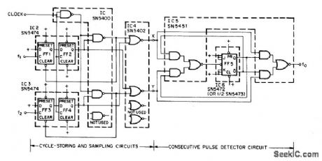
Can be used with wide range of dock frequencies up to 5.3 MHz to provide output frequency that is equal to absolute difference between input frequencies f1 and f2. Artide traces operation of circuit and gives design equations.—P. B. Morin, Frequency. Comparator Provides Difference Fre-quency, EEEMagazine, April 1971, p 65-66. (View)
View full Circuit Diagram | Comments | Reading(724)
60_W_WITH_DC_COUPLED_OUTPUT
Published:2009/6/29 1:39:00 Author:May
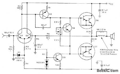
Q6 is Motorola MJE6044 complementary Darlington output transistor、and Q7 is MJE6041 Q1 and Q2 are MD8002 dual transistor,Q3 is MPS-A56, Q4 is MPS-A13 and Q5 is MPSA06.For 8-ohm loudspeaker suppiv is ±36V with 6.2K for R4、430 ohms for R5、and 33K for R7.output center oltage must be maintained at 0 VDC to ensuremaximum signal swing and prevent DC voltage from acting on loudspeaker, Frequency responseis 10 Hz to 50 kHz for -1 dB points,Samecircuit is used with different components for other powers down to 15 W and for 4-ohm loudspeaker,-R G,Ruehs,″15 to 60 Watt Audio Amplifiers Using Complementan Darlington Output Transistors,″ Motorola、 Phoenix, AZ 1974, AN-483B, p 5. (View)
View full Circuit Diagram | Comments | Reading(4085)
THERMOCOUPLE_AMPLIFIER
Published:2009/6/29 1:39:00 Author:May
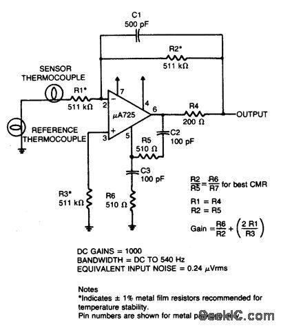
View full Circuit Diagram | Comments | Reading(2004)
1500v isolation circuit diagram of D/A convertor
Published:2011/7/30 9:39:00 Author:Sophia | Keyword: D/A convertor, 1500v isolation circuit
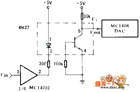
The circuit adopts the Motorola4N27 optical isolator, which provides the required isolation between programmable power D / A converter and CMOS MC1408 non-inverting buffers located far distance. (View)
View full Circuit Diagram | Comments | Reading(673)
FREQUENCY_PHASE_UP_TO_25_MHz
Published:2009/6/29 1:36:00 Author:May
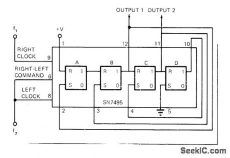
Universal shfft register such as 5495/7495 is connected to compare both frequency and phase of two carier signals anywhere in range from DC to 25 MHz. When f1 is greater than f2, output is 1; when f1 is less than f2, output is 0. For f1 = f2, output is square wave whose duty cycle varies linearly with phase difference between f1 and f2. Comparisons are almost instantaneous, requiring at most two carrier cycles.—J. Breese, Single IC Compares Frequencies and Phase, EDN Magazine, Sept, 15, 1972, p 44. (View)
View full Circuit Diagram | Comments | Reading(1461)
19_21_V_WINDOW_COMPARATOR
Published:2009/6/29 1:27:00 Author:May
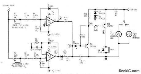
When positive input voltage is between Ievels set by R1 and R5, relay is actuated and green indicator lamp is turned on. Red lamp is on for voltages outside Iimits of window. Article gives design equations and traces operation of circuit. Number of components can be greatly reduced by changing opamps to LM111 comparators.—J.C. Nirschl, 'Window' Comparator Indicates System Status, EDN|EEE Magazine, June 15, 1971, p 49-50. (View)
View full Circuit Diagram | Comments | Reading(766)
INTERNALLY_GATED_WINDOW_COMPARATOR
Published:2009/6/29 1:25:00 Author:May
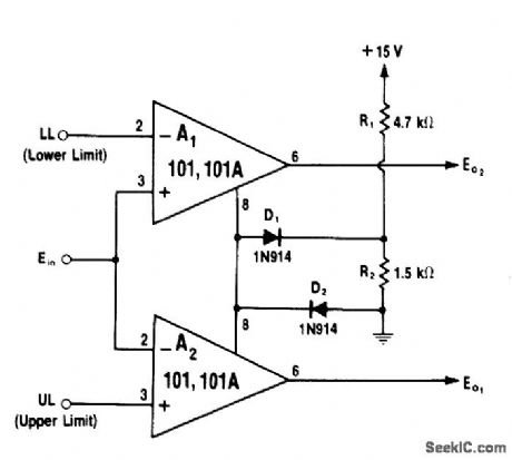
Operation is based on fact that source and sink currents available at pin 8 of 101 opamp are unequal, with negative-going drive being larger. Voltage at pin 8 is low if either comparison input (A1 or A2 so dictates. Both A1 and A2 must have high outputs for pin 8 to be high. Outputs of A1 and A2 thus follow pin 8 since opamps have unity gain. D1 and D2 form clamp network. Either output of A1 or A2 can be used. Outputs go to +5 V only when input voltage is in window established by upper and lower voltage limits.-W. G. Jung, IC Op-Amp Cookbook, Howard W, Sams, Indianapolis, IN, 1974, p 231-232. (View)
View full Circuit Diagram | Comments | Reading(846)
STAIRCASE_WINDOW_COMPARATOR
Published:2009/6/29 1:24:00 Author:May
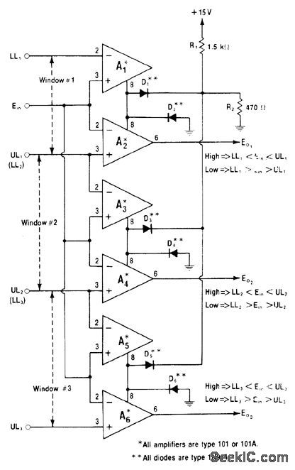
Cascading of 101-type window comparators for sequential operation indicates which of three windows input voltage is in. Input voltage is applied in parallel to all comparators. Output goes high only for comparator whose range includes voltage value of input. Lamp or other indicator can be added to each output line to give visual indication of voltage range.—W. G. Jung, IC Op-Amp Cookbook, Howard W. Sams, Indianapolis, IN, 1974, p 233-234. (View)
View full Circuit Diagram | Comments | Reading(1478)
5_V_CLAMPED_COMPARATOR
Published:2009/6/28 23:48:00 Author:May
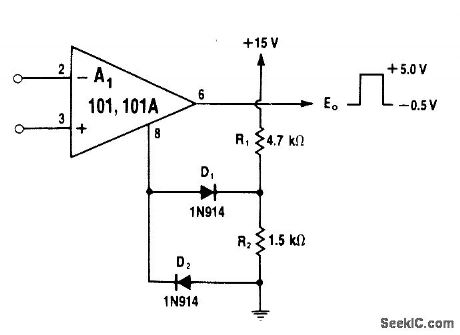


R1 and R2 provide +3.8V bias for D1,clamping positive outputof comparator opamp to +5 V,D2 limits negative output swing to-0.5V.Open-loop circuit means that output voltage will vary in proportion to load current.—W.G.Jung, IC Op-Amp Cookbook, Howard W.Sams,Indianapolis,IN、1974,p 226-228 (View)
View full Circuit Diagram | Comments | Reading(651)
CROSSOVER_FOR_20_Hz_SUBWOOFER
Published:2009/6/28 23:44:00 Author:May
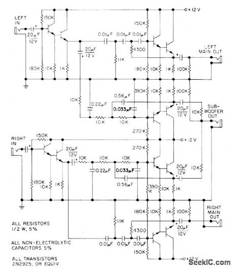
Used at channel outputs of stereo system when re-producing music down to 20 Hz as synthesized by electronic function generators. Active crossover network drives subwoof er (low-bass loudspeaker) connected in bridgedcenter configu-ration, for handling sounds below range of normal woofer. Crossover consists of thirdorder Butterworth (18 dB per octave) networks providing 20-Hz cutoff along with 100-Hz cross-over. Response of subwoofer should extend one octave above crossover. 0ne advantage of active crossover is freedom from transient intermodulation distortion.-W. J. J. Hoge, Switched-0n Bass, Audio, Aug. 1976, p 34-36, 38, and 40 (View)
View full Circuit Diagram | Comments | Reading(2390)
46_dB_GAlN
Published:2009/6/28 23:43:00 Author:May
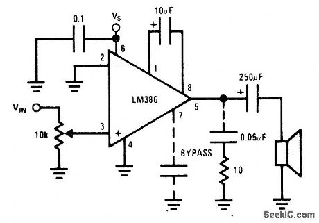
Single National LM386 power amplifier provides gain of 200 V/V at maximum output power of 250 mW for 12-V supply. Op-tional 0.05-μF capachor and 10-ohm resistor suppress bottomside oscillation occurring during negative swing into Ioad drawing high current.- Audio Handbook, National Semicon-ductor, Santa Clara, CA, 1977, p 4-30-4-33. (View)
View full Circuit Diagram | Comments | Reading(644)
1_W_CLASS_B
Published:2009/6/28 23:42:00 Author:May

Audio application of CA3020A wideband power amplifier provides 1-W outputto loudspeaker load through AF output transformer with 10% total harmonic distortion VCC1 is 9 V、and VCC2 is 12 V With CA3020 both supply voltages are 9V and maximum power output is 550 mW.Sensitivity is 35-45 mV,-″Linear Integrated Circuits and MOS/FET's,″RCASolid State Division,Somelville, NJ, 1977,p 105 (View)
View full Circuit Diagram | Comments | Reading(925)
MICROVOLT_COMPARATOR
Published:2009/6/28 23:42:00 Author:May
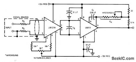
Combination of National LM121A preamp and LM111 comparator serves for comparing DC signal levels that are only within microvolts of each other. With bias network shown, preamp has open-loop temperature-stable voltage gain close to 100.Separation of preamp from comparator chip minimizes effects of temperature variations.Circuit hysteresis is 5 μV, which under certain conditions can be trimmed to 1 μV.— Linear Applications, Vol. 2, National Semiconductor, Santa Clara, CA, 1976, LB-32. (View)
View full Circuit Diagram | Comments | Reading(1236)
HEADPHONE_OPAMPS
Published:2009/6/28 23:42:00 Author:May
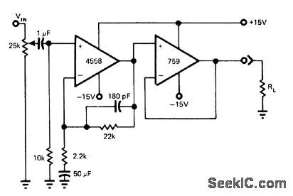
Dual low-noise 4558 opamp provides gain and reduces system noise and distortion, while 759 power opamp supplies output power of 0.7 W into 16-ohm load with Iessthan 0.170 total harmonicdistortion.-R. J. Apfel, Power Op Amps-Their Innovative Circuits and Packaging Provide Designers with More Options, EDN Magazine, Sept.5,1977, p 141-144. (View)
View full Circuit Diagram | Comments | Reading(4456)
OTA_single_control_function_generatorminimum_component
Published:2009/7/25 1:09:00 Author:Jessie
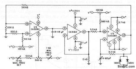
This circuit is similar to that of Fig.11-3,except that less components(and adjustments) are required.The frequency range is from 2 Hz to 1 MHz. (View)
View full Circuit Diagram | Comments | Reading(848)
Differential_to_single_ended_converter
Published:2009/7/25 1:07:00 Author:Jessie
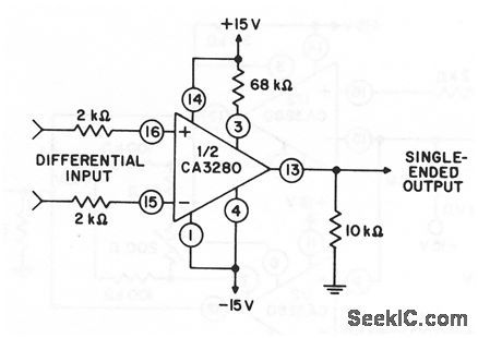
This circuit shows one section of an OTA connected to provide a single-ended output for a differential input. (View)
View full Circuit Diagram | Comments | Reading(1587)
STROBED_COMPARATOR
Published:2009/6/28 23:39:00 Author:May
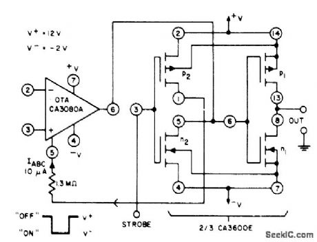
Combination of CA3080A opamp and two CMOS transistor pairs from CA3600E array gives programmable micropower comparator having quiescent power drain of about 10μW. When comparator is strobed on, opamp becomes activeand circuit draws 420μW while responding to differentialinput signalin about 8μs. Common-mode input range is -1 V to +10.5 V. Voltage gain of comparator is typically 130 dB.— Linear Integrated Circuits and MOS/FET's, RCA Solid State Division, Somerville, NJ, 1977, p 279. (View)
View full Circuit Diagram | Comments | Reading(831)
| Pages:144/250 At 20141142143144145146147148149150151152153154155156157158159160Under 20 |
Circuit Categories
power supply circuit
Amplifier Circuit
Basic Circuit
LED and Light Circuit
Sensor Circuit
Signal Processing
Electrical Equipment Circuit
Control Circuit
Remote Control Circuit
A/D-D/A Converter Circuit
Audio Circuit
Measuring and Test Circuit
Communication Circuit
Computer-Related Circuit
555 Circuit
Automotive Circuit
Repairing Circuit