
Index 146
LOW_COST_30_W
Published:2009/6/28 23:25:00 Author:May
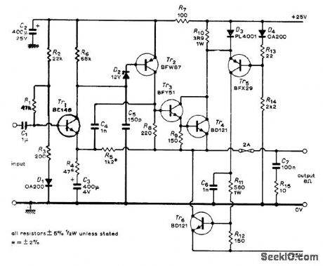
Economical compromise gives 30 W into 8-ohm load at 0.1% distortion (mainly second harmonic) and hum level of -50 dBW. Article covers design and operation of cir, cuit in detail.-P. L, Taylot, Audio Power Am-plifier, Wireless Wolld, June 1973, p 301-302, (View)
View full Circuit Diagram | Comments | Reading(640)
35_W_BRIDGE_AMPLIFIER
Published:2009/6/28 23:21:00 Author:May
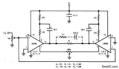
Bridge connection of National LM388 power opamps provides 3.5 W to 8-ohm loudspeaker when using 12-V supply. With 6-V supply and 4-ohm load, maximum power is 1 W. Coupling capacitors are not re quired since output DC levels are within several tenths of a volt of each other.- Audio Hand-book, National Semiconductor, Santa Clara, CA, 1977, p 4-37-4-41. (View)
View full Circuit Diagram | Comments | Reading(835)
HAMMER_DRIVER
Published:2009/6/28 23:21:00 Author:May
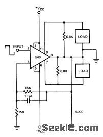
Signetics 540 power driver handles either push-pull or single-ended inductive loads such as relays, solenoids, motors, and electric hammers. In push-pull connection shown, load is driven in either positive, negative, or both arms of output. Either output can be selected by appropriate choice of input pulse polarity. Supply can be ±5 to ±25 V.- Signetics Analog Data Manual, Signetics, Sunnyvale, CA, 1977, p 764. (View)
View full Circuit Diagram | Comments | Reading(661)
30_W
Published:2009/6/28 23:20:00 Author:May
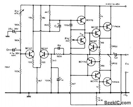
Designed for use with active filter crossover networks for three loudspeakers. For lowest-frequency channel, C3 is 150μF and C4 is 50μF. For middle channel, C3 and C4 are 25μF. For high-frequency channel, C3 and C4 are 10μF.Article includes circuit for active filter network.-D. C. Read, Active Filter Crossover Networks, Wireless World, Dec. 1973, p 574-576. (View)
View full Circuit Diagram | Comments | Reading(783)
COMPLEMENTARY_SYMMETRY_AMPLIFIER
Published:2009/6/28 23:13:00 Author:May
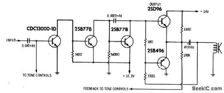
Simplified version of cicuit takes advantage of fact that PNP and NPN transistors require signais of opposite polatity to perform same function. Bases of output transistors are fed in parallel, with loudspeaker connected to common terminal of transistors. Drawback is difficulty of locating matched PNP and NPN transistors,-J. J. Carr, Solid-State Audio: A neview of the Latest Circuitry and General Troubleshooting Procedures, Electronic Servicing, Aug. 1971, p 38-43. (View)
View full Circuit Diagram | Comments | Reading(1260)
500_OHM_INPUT
Published:2009/6/28 23:12:00 Author:May
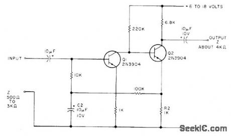
Simple audio amplifier having high gain, low noise, and excellent temperature stability can be used as mike booster, first AF amplifier stage in receiver, or for other preamp applications. With values shown, circult will amplify down to about 10 Hz. To increase low-frequency cutoff for speech amplifier, reduce 02 to 1μF or less.-E. Dusina, Build a General Purpose Preamp, 73 Magazine, Nov.1977,p 98. (View)
View full Circuit Diagram | Comments | Reading(1076)
BROADBAND_NOISE_AMPLIFIER
Published:2009/6/28 23:02:00 Author:May
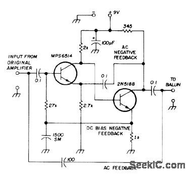
Developed for use with antenna noise bridges for measurements at 20 meters. Provides 35 to 50 dB additional gain, not entirely constant over use-ful range of 1.8 to 30 MHz. Three strong feedback loops are introduced between drivor and final amplifier Use transistors specified, because substitutions may cut overall gain by 10 to 20 dB.-A Weiss、Noise Bridge,Ham Radio,May 1974、p 71-72 (View)
View full Circuit Diagram | Comments | Reading(851)
The relay low-power maintenance
Published:2011/7/21 1:59:00 Author:Seven | Keyword: low-power, maintenance circuit
The pulling in current of the relay is high that its releasing current, when the relay pulls in, the relay will working while keeping the state. See as the figure, the circuit can make the relay working in a low current after it pulls in, so the power consumption is reduced. When the 3-pin of 555 is turned into the high LEV from the low, as the voltage on C can't mutate, so the input current that VT acquires is (VA-0.7V)/R2. After that, C is charged by R2 and eb Knot, VB is falling down, when C is full, VB=VA-Vc. (View)
View full Circuit Diagram | Comments | Reading(636)
The low-power timing switch circuit
Published:2011/7/21 2:06:00 Author:Seven | Keyword: low-power, timing switch
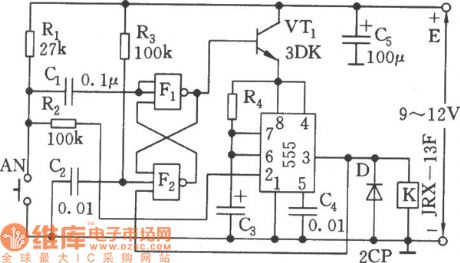
See as the figure, the timing circuit can reduce the 555 static current to l~2μA as it is fixed with the electric switch composed of F1, F2 and VT1. When the power supply is on, as the voltage on C2 can't mutate, so the F2 gate circuit is in a high LEV, the F1 output is located at a low LEV, VT1 is blocked, which makes the static current of the circuit low. When the timing switch AN is pressed, there is a negative pulse on the input terminal of F1, F1 outputs a high LEV, VT is conducting, then 555 has got a power supply voltage.
(View)
View full Circuit Diagram | Comments | Reading(708)
The sound control relay circuit
Published:2011/7/23 22:16:00 Author:Seven | Keyword: sound control relay
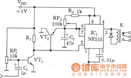
See as the figure, the circuit consists of the sound detection circuit and single steady trigger circuit, the relay is the executing component. VT1 finish the magnifying job of the input audio signal, when signals come, the 555 is reset, K is pulling in, VT2 is conducting, the electricity on C2 is released by the discharging tube and VT2 in 555. After the sound is gone, both VT1 and VT2 are blocked, C2 charges them through R2 and RP2, the contemporary stable time of the single stable circuit is td =1.1(R2+RP2)C2, the delaying time is 0.05~0.5S which can be adjusted by RP2. (View)
View full Circuit Diagram | Comments | Reading(958)
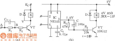
The industrial time relay circuit
Published:2011/7/21 1:51:00 Author:Seven | Keyword: time relay circuit
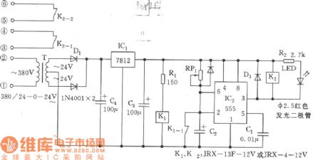
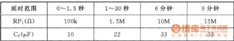
See as the figure, the time relay is to replace JSK, which is designed for the transistor time relay. The circuit includes the step-down regulated voltage source(+12V), 555 single stable circuit and relay control, etc. 555, RP1 and C2 compose the single stable delay circuit, the time td =l.1RP1C2. When the power supply is on, as the 2-pin is in a low LEV, the 555 is reset, K2 is still, when C2 is charged to 2/3VDD by RP1, 3-pin is in a low LEV, K2 is pulling in, which connects with the contactors of K2-1 and K2-2.
(View)
View full Circuit Diagram | Comments | Reading(652)
The D/A converter dual phase complementary frequency generator circuit
Published:2011/7/23 22:29:00 Author:Seven | Keyword: D/A converter, frequency generator
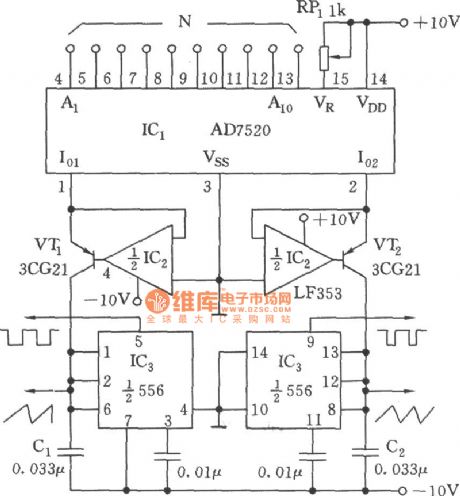
See as the figure, AD7520 is a CMOS 10-bit multi-channel DAC integrated circuit, which can provide with the output current Io1 in forward proportion to the digital input N, it can also provide with the current Io2 in proportion to the (1023-N). Both VT1 and VT2 with wide band dual op-amp LF353 provide with charge current for the capacitors of C1 and C2. When the charge current on C1 and C2 reaches threshold value LEV 2/3VDD, 556 is reset; C1 and C2 are both discharged by the discharging tube in the base plate, and its LEV is reduced to 1/3VDD.
(View)
View full Circuit Diagram | Comments | Reading(773)
The Schmidt trigger circuit
Published:2011/7/23 22:38:00 Author:Seven | Keyword: Schmidt trigger
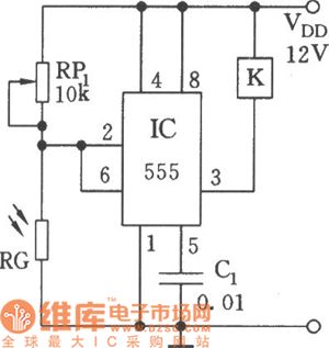
See as the figure, the circuit is based on 555, and 555 with LDR RG and RP1 composes the circuit. The resistance of RG changes with the light, by using the resetting and offsetting feature of the 2 comparators in 555, the Schmidt trigger is formed. When the light is strong, RG is in a low resistance, 2-pin is in low LEV(<1/3 VDD), 555 is offset, K is still; when the light is weak, RG is in a high resistance, 6-pin LEV is higher than 2/3VDD threshold LEV, 555 is reset, K is pulling in. (View)
View full Circuit Diagram | Comments | Reading(1084)
4 types of basic circuits of the single steady trigger composed of 555
Published:2011/7/24 1:43:00 Author:Seven | Keyword: single steady trigger, basic circuits
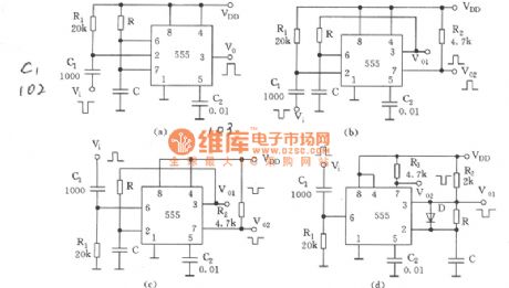
In Figure (a) is the typical single steady circuit. When an external pulse is added on the 2-pin of 555 after being past the C1 and R1 differential circuit, the forward pulse makes 555 offset, 3-pin is outputting a contemporary stable pulse width td=1.1RC. Figure b is like figure a, but it has 2 output terminals. C discharges the internal current of 555 through R, the recovering time is longer than that of Figure a. In figure c, the 2-pin and 6-pin of the circuit are different from figure a and figure b, the external trigger should be a forward pulse.
(View)
View full Circuit Diagram | Comments | Reading(695)
The single stable circuit with changeable width
Published:2011/7/21 3:26:00 Author:Seven | Keyword: stable circuit, changeable width
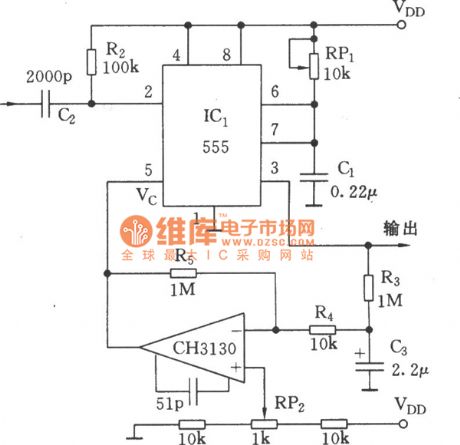
Usually, the single stable circuit outputs the solid pulse width. See as the figure, the circuit adopts the output pulse, after the pulse is low-pass filtered and DC amplified, the closed loop controls the 555 control terminal, the contemporary stable width will shrink automatically, so the cycle duty of the output waveform remains the same.
(View)
View full Circuit Diagram | Comments | Reading(632)
The low power single stable circuit
Published:2011/7/21 3:33:00 Author:Seven | Keyword: low power, single stable circuit
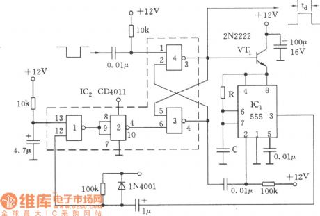
See as the figure, the circuit contains a 2-input terminal NAND CD4011 and a CMOS 555, so whether it is static or high LEV output timing period, the consuming power is very low. The door 3 and 4 of CD4011 compose the RS trigger. As the whole circuit is a closed circuit, the time pulse width is decided by the RC time constant, i.e td=1.1R1C1. (View)
View full Circuit Diagram | Comments | Reading(641)
The duty cycle adjustable square wave generator circuit composed of 555
Published:2011/7/24 1:51:00 Author:Seven | Keyword: duty cycle, square wave generator
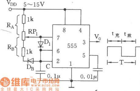
Once the circuit was added with a voltage VDD, the oscillator would start the oscillate. When the circuit is connected, as the voltage on C can't mutate, i.e the 2-pin LEV is the earth LEV firstly, which makes 555 offset, 3-pin is in a high LEV. C charges the generator through RA and D1, the charge time is tc=0.693RAC, when the voltage on C rises to 2/3VDD, 555 is reset, 3-pin is in a low LEV, at this moment, C discharge with the help of D1, R8 and the discharge tube in 555, the discharge time is td=0.693RbC. (View)
View full Circuit Diagram | Comments | Reading(2635)
The tone changeable multivibrator circuit
Published:2011/7/24 1:57:00 Author:Seven | Keyword: tone changeable multivibrator, circuit

This tone changeable multivibrator circuit consists of the time-based circuit 555, which can emit the continuous changing oscillating wave of 400~2500Hz, like the police car sound. The circuit consists of the starting relay, low-frequency oscillator and modulating audio generator. (View)
View full Circuit Diagram | Comments | Reading(741)
A digital power amplifier circuit diagram
Published:2011/7/31 22:11:00 Author:Ecco | Keyword: digital power amplifier
View full Circuit Diagram | Comments | Reading(658)
5.1ch amplifier circuit diagram
Published:2011/7/31 22:10:00 Author:Ecco | Keyword: 5.1ch amplifier
View full Circuit Diagram | Comments | Reading(8245)
| Pages:146/250 At 20141142143144145146147148149150151152153154155156157158159160Under 20 |
Circuit Categories
power supply circuit
Amplifier Circuit
Basic Circuit
LED and Light Circuit
Sensor Circuit
Signal Processing
Electrical Equipment Circuit
Control Circuit
Remote Control Circuit
A/D-D/A Converter Circuit
Audio Circuit
Measuring and Test Circuit
Communication Circuit
Computer-Related Circuit
555 Circuit
Automotive Circuit
Repairing Circuit