
Index 192
ACTIVE_LOAD
Published:2009/7/12 22:24:00 Author:May
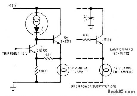
National NSL4944 constantcurrent LED serves as cuffent source for collector resistor of Schmitt trigger to provide up to 12-V output at 40 mA for lamp load. When lamp andQ2 are off, most of LED current flows through 100-ohm resistor to determine circuit trip point of 2 V. When control signal saturates Q1, Q2 provides about 1 V for lamp to give some preheating and reduce starting cument surge.When control is above trip point, Q2 tums on and energizes lamp.-''Linear Applications, Vol.2,''National Semiconductor,Santa Clara, CA,1976,AN-153,P 3.
(View)
View full Circuit Diagram | Comments | Reading(1006)
FILAMENT_EMISSION_REGULATOR
Published:2009/7/12 22:24:00 Author:May
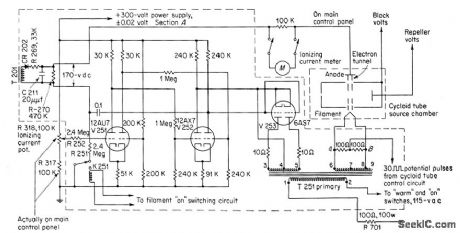
Used in Consolidated Electrodynamics gas analyzer to control ionizing current strength by regulating filament temperature of cycloid tube Potentiometer used for control is in grid circuit of V251. Circuit maintains ionizing current automaticcdly at desired level-G.C.Carroll, Industrial Instrumenl Servicing Handbook, McGraw-Hill,N,Y,1960,p8-122 (View)
View full Circuit Diagram | Comments | Reading(700)
ACQUISITION_RELAY_DRIVER
Published:2009/7/12 22:22:00 Author:May
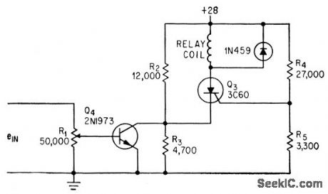
Scr Q3 and transistor Q4 provide stable triggering point for acquisition signal used in aligning missile guidance systems, without hysteresis effect.-W.S. Zukowsky, Aligning Saturn Missile's Guidance System, Electronics, 37:8, p26-27. (View)
View full Circuit Diagram | Comments | Reading(712)
The biphasic pulse generator circuit composed of CD4013
Published:2011/8/4 8:20:00 Author:nelly | Keyword: biphasic pulse, generator
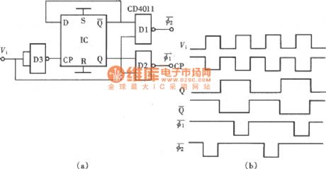
Inthedesignofthedigitalcircuit,wemayneedapairofbiphasicpulsegenerators.ThebiphasicpulsegeneratorcomposedofCD4013isasshown.(a)isschematic,and(b)isthewaveform. (View)
View full Circuit Diagram | Comments | Reading(2958)
delay relay circuit composed by LM122
Published:2011/7/26 9:18:00 Author:Nancy | Keyword: delay relay
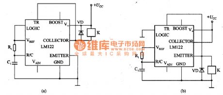
Figure 1 is the delay relay circuit composed by LM122. The LM122 is a timer integrated circuit from microsecond to hour level with a constant voltage circuit inside, so the timing is not effected by the change of the supply voltage, the output current is 50 mA and the working voltage is from 4.5 to 40 V.
The Figure 1 (a) is a relay K energization circuit after the RtCt timing. When the relay loses electric, the external voltage +Ucc is off. The Figure 1 (b) shows that the relay K conducts and works with external voltage +Ucc and disconnects after the RtCt timing. The relay is off when you cut off the power again until the next operation. (View)
View full Circuit Diagram | Comments | Reading(800)
Quantitative Pulse Output Circuit With CD4046
Published:2011/8/4 8:25:00 Author:nelly | Keyword: Quantitative Pulse, Output
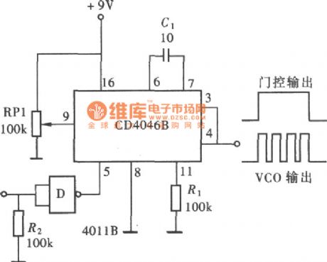
Quantitative Pulse Output Circuit With CD4046 is as shown (View)
View full Circuit Diagram | Comments | Reading(2397)
0.1Hz~500kHz signal source circuit made by LM567
Published:2011/8/4 8:36:00 Author:nelly | Keyword: signal source
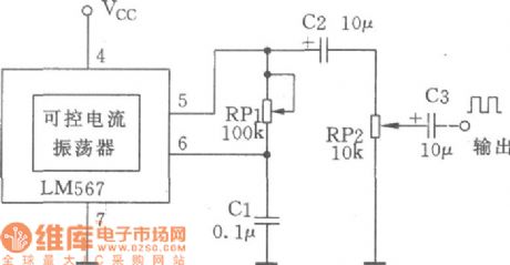
Manifold block LM567 is the high stability phase-locked loop circuit which has the phase-locked loop circuit. Using the internal “controllable current oscillator” of this manifold block can make a simple adjustable low-frequency signal source, so the maintenance will be very convenient. The circuit is as shown.
(View)
View full Circuit Diagram | Comments | Reading(1369)
Multipurpose FM Signal Generator Circuit
Published:2011/8/4 8:54:00 Author:nelly | Keyword: Multipurpose, FM , Signal Generator
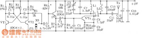
The figure is the multipurpose FM signal generator circuit. VTl and VT2 form the multivibrator. VT3 is the emitter-follower, which is used to modulate the signal source of VT4 oscillator. Then the signal will be emitted by Tx antenna. (View)
View full Circuit Diagram | Comments | Reading(741)
Pulse width modulation circuit (555)
Published:2011/8/4 8:29:00 Author:nelly | Keyword: Pulse width, modulation
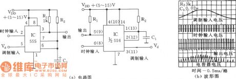
(a) circuit diagram (2)waveform (View)
View full Circuit Diagram | Comments | Reading(738)
FREEZER_SENTRY
Published:2009/7/12 22:19:00 Author:May
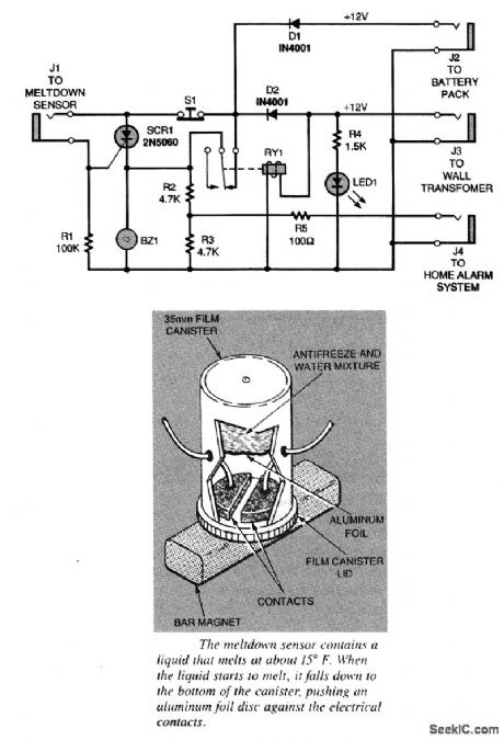
The heart of the circuit is SCR1, a silicon-controlled rectifier. Trigger voltage is supplied through J1 by the meltdown sensor when its contacts close. Resistor R1 is included to prevent any false triggering of SCR1 as a result of voltage fluctuations or noise from the power supply. Once SCR1 is triggered, it latches on, sounding the alarm buzzer until the reset switch (S1) is pressed. The reset switch interrupts current flow through the SCR, letting it turn off. Power for the circuit is supplied by a 12-Vdc wallmounted transformer, which is connected to J3. As long as the wall-mounted power supply is working, relay RY1 will be activated, opening its normally closed contact. Normal power will also be indicated by LED1, withR4 limiting the current flowthrough the light-emitting diode. If the ac powerfails, LED1 will go out and RY1 will deenergize, closing the relay's normally closed contacts. The relay contacts bypass SCR1, sounding the alarm. Backup power for that situation is supplied by a 12-V battery pack, which is connected to the circuit through J2 and D1. Diode D1 prevents the ac-derived power supply from attempting to charge the batteries, and D2 prevents the batteries from lighting the LED or energizing RY1 in the event of ac power failure. An additional feature of the circuit is that since the relay bypasses SCR1 during a loss of ac power, the reset button will not silence the alarm. Regardless of which type of failure caused the alarm to sound, R2 and R3 form a voltage divider that provides a 5-V signal to J4. (View)
View full Circuit Diagram | Comments | Reading(950)
TIME_DELAY_USES_POWER_TRANSISTOR_IC
Published:2009/7/12 22:16:00 Author:May
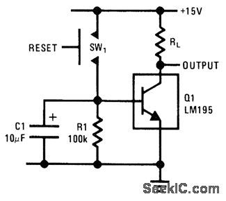
Load is energized when switch is closed C1 charges until voltage across R1 drops below 0.8V、opening LM195 and deenergizing load,Long time delays can be obtained with small capacltor values since high resistance can be used.- Linear Applications,vol 2, National Semiconductor.Santa Clara, CA, 1976,AN-110,p 4. (View)
View full Circuit Diagram | Comments | Reading(875)
CASCADE_WITH_AUTOMATIC_RETRIGGERING
Published:2009/7/12 22:15:00 Author:May
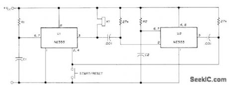
Two timers, each controlling own load andhaving own time intervals (determined by R1C1 and R2C2), recycle automatically when start switch is closed momentarily. If desired, second timer can be set to control ON time offirst timer With 15-V supply, each timer canhandle 200-mA load.-H .Vordenbaum'Automatic Beset Timer,Ham Radio Oct,1974、p50-51. (View)
View full Circuit Diagram | Comments | Reading(650)
SPLITTER_CIRCUIT_FOR_ACTIVE_ANTENNA_TO_ENABLE_MULTIPLE_SHORTWAVE
Published:2009/7/12 22:14:00 Author:May
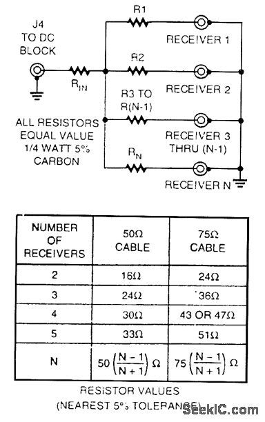
Identical resistor-value star networks can beused to connect multiple receivers to a single active antenna Although the loss is higher with this method than with conventional ferrite transformersplitters,the frequency response goes down to dc.and the extra loss is not usually a problem at LF,MF, and HF, as active antennas have plenty of gain and the received signal levels are limited by at mospherig and ambient noIse signal strengths.The splitter should be mounted in a shielded box with suitable connectors to minimize stray signal pickup. (View)
View full Circuit Diagram | Comments | Reading(880)
5_V_SUPPLY_FROM_THREE_WIRE_RS232_PORT
Published:2009/7/12 22:14:00 Author:May
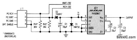
This circuit produces a semiregulated 5-V output from an RS232 port. The output current-about 8 mA-is sufficient for CMOS microcontrollers and other low-power circuits. IC1 is a switched-capacitor, charge-pump voltage converter that can either invert an input voltage or double it. The connections shown provide a doubler configuration in which the normal input voltage is reversed: A positive input voltage normally connects between GND and OUT, but this circuit connects a negative input between OUT and GND. The IC then doubles the negative Vin the positive direction, producing a positive output (at VDD) equal to [Vin]. The zener diode D1 acts as a shunt regulator that semiregulates Vin to -5 V (actually to -4.7 V). The 33-μF capacitor values shown are larger than normal to support the oqtput voltage during worst-case (all-zero) patterns of transmission. At 9600 baud, for example, an all-zeros character causes an output droop of about 0.2 V. For lower baud rates, substitute a proportionally higher value for C1. (View)
View full Circuit Diagram | Comments | Reading(670)
DC_BLOCK_FOR_ACTIVE_ANTENNA_AND_DOWNCONVERTERS
Published:2009/7/12 22:13:00 Author:May
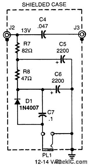
A suitable dc block and power source for active antennas and downconverters can be made from a few components as shown. This circuit is suitable for frequencies from 50 kHz up to VHF. A shielded case should be employed to prevent stray signal pickup. Dc power supplied to the active antenna or downconverter, via the coaxial signal ca-ble, is 12 V at 30 mA. (View)
View full Circuit Diagram | Comments | Reading(697)
ACTIVE_ANTENNA,100_kHz_TO_30_MHz
Published:2009/7/12 22:12:00 Author:May
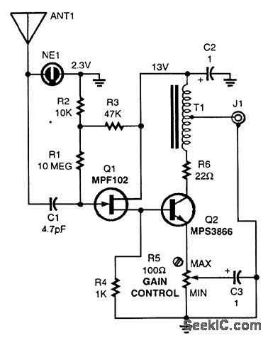
This circuit uses a FET and bipolar transistor combination to achieve high performance with a short pickup antenna (24 in. or 70 cm). R5 is a gain control and should be set for the minimum gain necessary for good results. T1 is 24 turns of #32 trifilar wire on a Ferroxcube P/N 768T188-3E2A core. J1 is used for dc feed and RE output. A dc block unit can be used at the receiver end. Dc power is 12 V at 30 mA. The pickup wire and pre-amp should be enclosed in a weatherproof assem-bly so that the antenna can be mounted outdoors in an electrically quiet area.A complete kit of parts, including the PC board, is available from North Country Radio, P.O. Box 53, Wykagyl Station, New Rochelle, NY 10804-0053A.
(View)
View full Circuit Diagram | Comments | Reading(1441)
10_h_DELAYS
Published:2009/7/12 22:12:00 Author:May
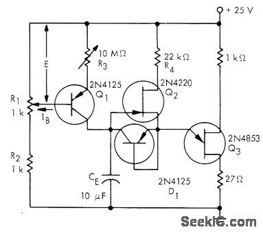
Long duration is achieved by separating peak current of timer from charging cuffent. Q1 and R1-R2-R3 form constant-current source whose charging current can be ad justed to as low as several nanoamperes. Q2 acts as source follower to supply current flowing in emitter lead priorto firing of UJT Q3. Diode-con-nected transistor Q1 provides low-impedance discharge path for timing capacitor CE. Delay time varies linearly with setting of R3.- Uni-junction Transistor Timers and Oscillators, Motorola, Phoenix, AZ, 1974, AN-294, p 5. (View)
View full Circuit Diagram | Comments | Reading(639)
12_V_TRANSFORMERLESS_PRENEGULATOR
Published:2009/7/12 22:11:00 Author:May
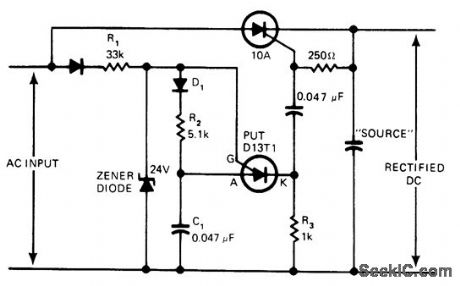
AC line voltage is converted to regulated 12 VDC by varying firing angle of 10-A SCR. Circuit provides reliable operation for AC line voltages between 50 and 140 V. Key element in trigger-ing of SCR is programmable unijunction transistor that provides variable and accurate control of firing time. Developed for use in power supply that uses digital techniques of sample-and-hold switching to achieve high degrbe of isolation between power line and load without using transformer.-J. A. Dickerson, Transformerless Power Supply Achieves Line-to-Load isolation, EDN Magazine, May 5, 1976, p 92-96. (View)
View full Circuit Diagram | Comments | Reading(2377)
PC_IR_CARD_READER
Published:2009/7/12 22:10:00 Author:May
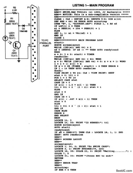
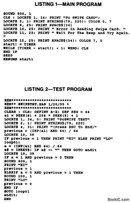
The LED is a high-output infrared emitter. It receives its power through current-limiting resistor R1. With a 9-V power supply and a value of 220 Ω for R1, the diode will receive about 25 mA of current. With a 5-V supply, R1 should be 150 Ω to keep diode current in the 25-mA range. The LED energizes NPN phototransistor Q1, which is configured as a simple inverting amplifier. As more light shines on Q1, the output voltage at its collector decreases. With a value of 2.2 kΩ for R2, the circuit provides TTL-compatible logic levels. The output of Q1 feeds one bit of a PC's parallel port. Diode D2 allows the use of power sources greater than 5 V, thereby maintaining TTL level compatibility-even with high supply voltages. If the voltage at the collector of Q1 ever exceeds 5 V, D2 will block the voltage, thereby protecting the port. On the other hand, when Q1 goes logic low, D2 becomes forward-biased, so the low level can be sensed by the port. (View)
View full Circuit Diagram | Comments | Reading(667)
MAGENTIC_REGISTER
Published:2009/7/12 22:10:00 Author:May
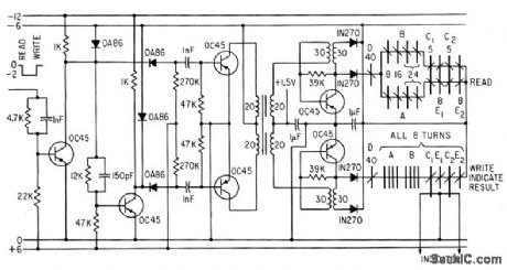
Basis of storage is magetization time.Four ferrite cores will store one deciaml digit under control of one clock pulse.-A.A.Jaecklin.Storing Complete Decimal Digits with One Clock Pulse,Electronice,34:11,p50-53 (View)
View full Circuit Diagram | Comments | Reading(565)
| Pages:192/471 At 20181182183184185186187188189190191192193194195196197198199200Under 20 |
Circuit Categories
power supply circuit
Amplifier Circuit
Basic Circuit
LED and Light Circuit
Sensor Circuit
Signal Processing
Electrical Equipment Circuit
Control Circuit
Remote Control Circuit
A/D-D/A Converter Circuit
Audio Circuit
Measuring and Test Circuit
Communication Circuit
Computer-Related Circuit
555 Circuit
Automotive Circuit
Repairing Circuit